PCM1808
www.ti.com
SLES177A–APRIL 2006–REVISED AUGUST 2006
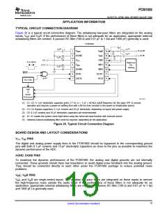
APPLICATION INFORMATION (continued)
VREF PIN
To ensure low source impedance of the ADC references, 0.1-µF ceramic and 10-µF electrolytic capacitors are
recommended between VREF and AGND. These capacitors should be located as close as possible to the VREF
pin to reduce dynamic errors on the ADC references.
DOUT PIN
The DOUT pin has a large load-drive capability, but if the DOUT line is long, locating a buffer near the PCM1808
and minimizing load capacitance is recommended to minimize the digital-analog crosstalk and maximize the
dynamic performance of the ADC.
SYSTEM CLOCK
The quality of the system clock can influence dynamic performance, as the PCM1808 operates based on a
system clock. Therefore, it may be necessary to consider the system clock duty, jitter, and the time difference
between system clock transition and BCK or LRCK transition in slave mode.
20
Submit Documentation Feedback

 BB [ BURR-BROWN CORPORATION ]