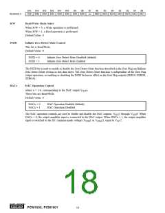
corresponds to the 8 data bits of the register indexed by the
REG[6:0] bits of Control Register 11. The Read cycle is
completed when ML is set to ‘1’, immediately after the MC
clock cycle for the least significant bit of indexed control
register has completed.
pin. The Read cycle starts by setting the R/W bit of the
control word to ‘1’, and setting all of the IDX[6:0] bits to
‘0.’. All subsequent bits input on the MDI are ignored while
ML is set to ‘0.’ For the first 8 clocks of the Read cycle,
MDO is set to a high-impedance state. This is followed by
a sequence of 8-bit words, each corresponding the data
contained in Control Registers 1 through N, where N is
defined by the REG[6:0] bits in Control Register 11. The
Read cycle is completed when ML is set to ‘1’, immediately
after the MC clock cycle for the least significant bit of
Control Register N has completed.
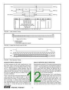
AUTO-INCREMENT READ OPERATION
The Auto-Increment Read function allows for multiple reg-
isters to be read sequentially. The Auto-Increment Read
function is enabled by setting the INC bit of Control Register
11 to ‘1’. The sequence always starts with Register 1, and
ends with the register indexed by the REG[6:0] bits in
Control Register 11.
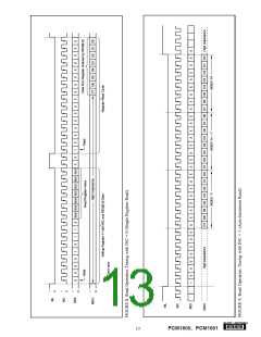
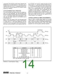
CONTROL INTERFACE TIMING REQUIREMENTS
Figure 10 shows a detailed timing diagram for the Serial
Control interface. Pay special attention to the setup and hold
times, as well as tMLS and tMLH, which define minimum delays
between edges of the ML and MC clocks. These timing
parameters are critical for proper control port operation.
Figure 9 shows the timing for the Auto-Increment Read
operation. The operation begins by writing Control Register
11, setting INC to ‘1’ and setting REG[6:0] to the last
register to be read in the sequence. The actual Read opera-
tion starts on the next HIGH to LOW transition of the ML
tMHH
50% of VDD
ML
tMLS
tMCH
tMCL
tMLH
50% of VDD
MC
tMCY
LSB
MDI
50% of VDD
tMDS
tMCH
tMOS
LSB
50% of VDD
MDO
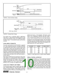
SYMBOL
PARAMETER
MIN
MAX
UNITS
tMCY
tMCL
tMCH
tMHH
tMLS
tMLH
tMDI
MC Pulse Cycle Time
MC Low Level Time
MC High Level Time
ML High Level Time
100
50
ns
ns
ns
ns
ns
ns
ns
ns
ns
50
300
20
ML Falling Edge to MC Rising Edge
ML Hold Time(1)
20
Hold Time
15
tMDS
tMOS
MDL Set Up Time
20
MC Falling Edge to MDSO Stable
30
NOTE: (1) MC rising edge for LSB to ML rising edge.
FIGURE 10. Control Interface Timing.
®
14
PCM1600, PCM1601

 BB [ BURR-BROWN CORPORATION ]