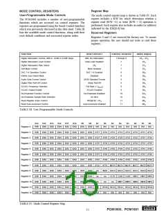
Register Map
MODE CONTROL REGISTERS
User-Programmable Mode Controls
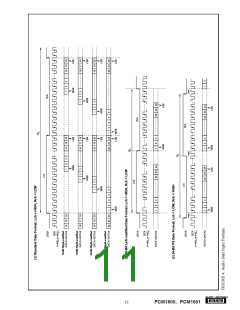
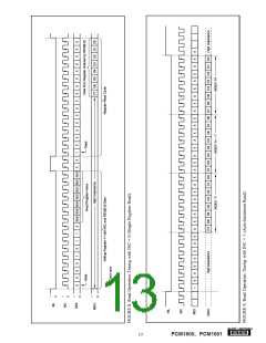
The mode control register map is shown in Table IV. Each
register includes a R/W bit, which determines whether a
register read (R/W =1) or write (R/W = 0) operation is
performed. Each register also includes an index (or address)
indicated by the IDX[6:0] bits.
The PCM1600 includes a number of user-programmable
functions which are accessed via control registers. The
registers are programmed using the Serial Control Interface
which was previously discussed in this data sheet. Table III
lists the available mode control functions, along with their
reset default conditions and associated register index.
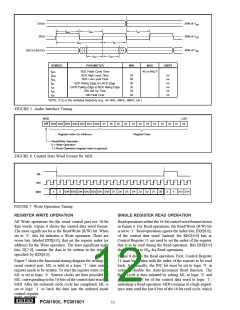
Reserved Registers
Registers 0 and 12 are reserved for factory use. To ensure
proper operation, the user should not write or read these
registers.
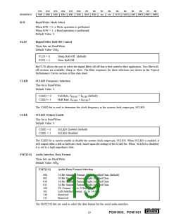
FUNCTION
RESET DEFAULT
CONTROL REGISTER
INDEX, IDX[6:0]
Digital Attenuation Control, 0dB to –63dB in 0.5dB Steps
Digital Attenuation Load Control
Digital Attenuation Rate Select
Soft Mute Control
0dB, No Attenuation
Data Load Disabled
2/fS
1 through 6
01H - 07H
07H
7
7
07H
Mute Disabled
DAC 1-6 Enabled
Disabled
7
07H
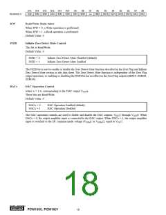
DAC 1-6 Operation Control
8
08H
Infinite Zero Detect Mute
8
08H
Audio Data Format Control
24-Bit Standard Format
Sharp Roll-Off
9
09H
Digital Filter Roll-Off Control
SCLKO Frequency Selection
SCLKO Output Enable
9
09H
Full Rate (= fSCLKI
)
9
09H
SCLKO Enabled
9
09H
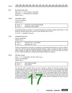
De-Emphasis Function Control
De-Emphasis Sample Rate Selection
Read Register Index Control
De-Emphasis Disabled
44.1kHz
10
10
11
11
0AH
0AH
0BH
0BH
REG[6:0] = 01H
Read Auto-Increment Control
Auto-Increment Disabled
TABLE III. User-Programmable Mode Controls.
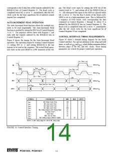
B15
R/W
B14
B13
B12
B11
B10
B9
B8
B7
B6
B5
B4
B3
B2
B1
B0
Register 0
Register 1
Register 2
Register 3
Register 4
Register 5
Register 6
IDX6
IDX5
IDX4
IDX3
IDX2
IDX1
IDX0
N/A
N/A
N/A
N/A
N/A
N/A
N/A
N/A
R/W
R/W
R/W
R/W
R/W
R/W
IDX6
IDX6
IDX6
IDX6
IDX6
IDX6
IDX5
IDX5
IDX5
IDX5
IDX5
IDX5
IDX4
IDX4
IDX4
IDX4
IDX4
IDX4
IDX3
IDX3
IDX3
IDX3
IDX3
IDX3
IDX2
IDX2
IDX2
IDX2
IDX2
IDX2
IDX1
IDX1
IDX1
IDX1
IDX1
IDX1
IDX0
IDX0
IDX0
IDX0
IDX0
IDX0
AT17
AT27
AT37
AT47
AT57
AT67
AT16
AT26
AT36
AT46
AT56
AT66
AT15
AT25
AT35
AT45
AT55
AT65
AT14
AT24
AT34
AT44
AT54
AT64
AT13
AT23
AT33
AT43
AT53
AT63
AT12
AT22
AT32
AT42
AT52
AT62
AT11 AT10
AT21 AT20
AT31 AT30
AT41 AT40
AT51 AT50
AT61 AT60
Register 7
Register 8
Register 9
Register 10
Register 11
Register 12
R/W
R/W
R/W
R/W
R/W
R/W
IDX6
IDX6
IDX6
IDX6
IDX6
IDX6
IDX5
IDX5
IDX5
IDX5
IDX5
IDX5
IDX4
IDX4
IDX4
IDX4
IDX4
IDX4
IDX3
IDX3
IDX3
IDX3
IDX3
IDX3
IDX2
IDX2
IDX2
IDX2
IDX2
IDX2
IDX1
IDX1
IDX1
IDX1
IDX1
IDX1
IDX0 ATLD ATTS MUT6 MUT5 MUT4 MUT3 MUT2 MUT1
IDX0
IDX0
IDX0
IDX0
IDX0
res
res
res
INC
N/A
INZD DAC6 DAC5 DAC4 DAC3 DAC2 DAC1
res
res
FLT0 CLKD CLKE FMT2 FMT1 FMT0
res DMF1 DMF0 DM56 DM34 DM12
REG6 REG5 REG4 REG3 REG2 REG1 REG0
N/A N/A N/A N/A N/A N/A N/A
TABLE IV. Mode Control Register Map.
®
15
PCM1600, PCM1601

 BB [ BURR-BROWN CORPORATION ]