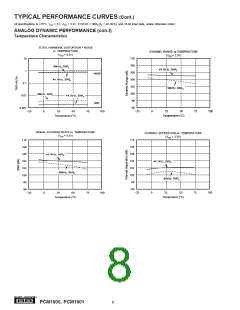
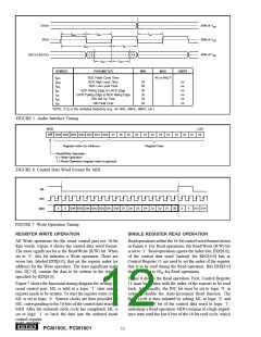
LRCK
BCK
50% of VDD
50% of VDD
tBCH
tBCL
tLB
tBCY
tBL
50% of VDD
DATA1-DATA3
tDS
tDH
SYMBOL
PARAMETER
MIN
MAX
UNITS
(1)
tBCY
tBCH
tBCL
tBL
BCK Pulse Cycle Time
BCK High Level Time
BCK Low Level Time
48 or 64fS
50
50
30
30
30
20
ns
ns
ns
ns
ns
ns
BCK Rising Edge to LRCK Edge
LRCK Falling Edge to BCK Rising Edge
DIN Set Up Time
tLB
tDS
tDH
DIN Hold Time
NOTE: (1) fS is the sampling frequency (e.g., 44.1kHz, 48kHz, 96kHz, etc.)
FIGURE 5. Audio Interface Timing.
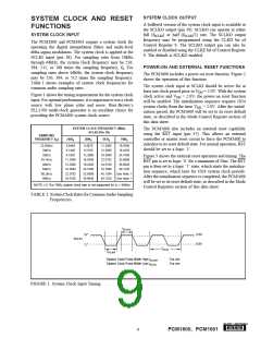
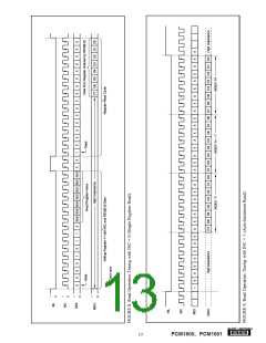
MSB
LSB
R/W IDX6 IDX5 IDX4 IDX3 IDX2 IDX1 IDX0
D7
D6
D5
D4
D3
D2
D5
D4
D3
D2
D1
D0
Register Index (or Address)
Register Data
Read/Write Operation
0 = Write Operation
1 = Read Operation (register index is ignored)
FIGURE 6. Control Data Word Format for MDI.
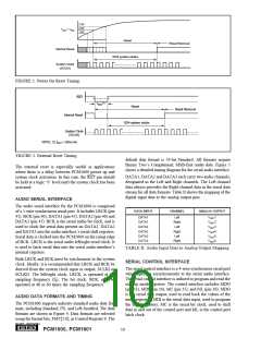
ML
MC
MDI
X
0
IDX6 IDX5 IDX4 IDX3 IDX2 IDX1 IDX0 D7 D6 D5
D4 D3 D2 D1 D0
X
X
D15 D14
FIGURE 7. Write Operation Timing.
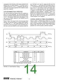
REGISTER WRITE OPERATION
SINGLE REGISTER READ OPERATION
All Write operations for the serial control port use 16-bit
data words. Figure 6 shows the control data word format.
The most significant bit is the Read/Write (R/W) bit. When
set to ‘0’, this bit indicates a Write operation. There are
seven bits, labeled IDX[6:0], that set the register index (or
address) for the Write operation. The least significant eight
bits, D[7:0], contain the data to be written to the register
specified by IDX[6:0].
Read operations utilize the 16-bit control word format shown
in Figure 6. For Read operations, the Read/Write (R/W) bit
is set to ‘1’. Read operations ignore the index bits, IDX[6:0],
of the control data word. Instead, the REG[6:0] bits in
Control Register 11 are used to set the index of the register
that is to be read during the Read operation. Bits IDX[6:0]
should be set to 00H for Read operations.
Figure 8 details the Read operation. First, Control Register
11 must be written with the index of the register to be read
back. Additionally, the INC bit must be set to logic ‘0’ in
order to disable the Auto-Increment Read function. The
Read cycle is then initiated by setting ML to logic ‘0’ and
setting the R/W bit of the control data word to logic ‘1’,
indicating a Read operation. MDO remains at a high-imped-
ance state until the last 8 bits of the 16-bit read cycle, which
Figure 7 shows the functional timing diagram for writing the
serial control port. ML is held at a logic ‘1’ state until a
register needs to be written. To start the register write cycle,
ML is set to logic ‘0’. Sixteen clocks are then provided on
MC, corresponding to the 16-bits of the control data word on
MDI. After the sixteenth clock cycle has completed, ML is
set to logic ‘1’ to latch the data into the indexed mode
control register.
®
12
PCM1600, PCM1601

 BB [ BURR-BROWN CORPORATION ]