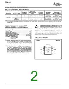
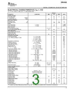
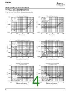
ꢂꢀꢉꢠ ꢡꢢ ꢣ
www.ti.com
SBOS286A − DECEMBER 2003 − REVISED SEPTEMBER 2006
changing the values of R1 and R2. The feedback resistor
values (R3 and R4) should be kept relatively low, as
indicated, for best noise performance.
APPLICATIONS INFORMATION
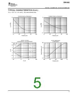
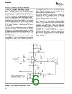
Figure 1 shows the OPA1632 used as a differential-output
driver for the PCM1804 high-performance audio ADC.
R5, R6, and C3 provide an input filter and charge glitch
reservoir for the ADC. The values shown are generally
satisfactory. Some adjustment of the values may help
optimize performance with different ADCs.
Supply voltages of 15V are commonly used for the
OPA1632. The relatively low input voltage swing required
by the ADC allows use of lower power-supply voltage, if
desired. Power supplies as low as 8V can be used in this
application with excellent performance. This reduces
power dissipation and heat rise. Power supplies should be
bypassed with 10µF tantalum capacitors in parallel with
0.1µF ceramic capacitors to avoid possible oscillations
and instability.
It is important to maintain accurate resistor matching on
R1/R2 and R3/R4 to achieve good differential signal
balance. Use 1% resistors for highest performance. When
connected for single-ended inputs (inverting input
grounded, as shown in Figure 1), the source impedance
must be low. Differential input sources must have
well-balanced or low source impedance.
The VCOM reference voltage output on the PCM1804 ADC
provides the proper input common-mode reference
voltage (2.5V). This VCOM voltage is buffered with op amp
A2 and drives the output common-mode voltage pin of the
OPA1632. This biases the average output voltage of the
OPA1632 to 2.5V.
Capacitors C1, C2, and C3 should be chosen carefully for
good distortion performance. Polystyrene, polypropylene,
NPO ceramic, and mica types are generally excellent.
Polyester and high-K ceramic types such as Z5U can
create distortion.
The signal gain of the circuit is generally set to
approximately 0.25 to be compatible with commonly-used
audio line levels. Gain can be adjusted, if necessary, by
V+
+8V to +16V
µ
10 F
+
µ
0.1 F
R3
Ω
270
C1
1nF
R1
R5
Ω
1k
3
Ω
40
8
2
1
5
+
Balanced or
Single−Ended
Input
VOCM
C3
2.7nF
1/2
PCM1804
R2
OPA1632
Ω
1k
−
4
6
R6
VCOM
(2.5V)
C2
1nF
7
Ω
40
R4
Ω
270
Enable(1)
OPA134
Ω
1k
µ
0.1 F
NOTE: (1) Leave open to enable.
µ
0.1 F
−
Logic signals referenced to V supply.
µ
10 F
See the Shutdown Function section.
+
−
−
−
8V to 16V
V
Figure 1. ADC Driver for Professional Audio
6

 BB [ BURR-BROWN CORPORATION ]