ꢂ
ꢀ
ꢉ
ꢠ
ꢡ
ꢢ
ꢣ
www.ti.com
SBOS286A − DECEMBER 2003 − REVISED SEPTEMBER 2006
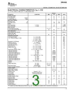
ELECTRICAL CHARACTERISTICS: V = 15V
S
V
= 15V: R = 390Ω, R = 800Ω, and G = +1, unless otherwise noted.
F L
S
OPA1632
PARAMETER
CONDITIONS
MIN
TYP
MAX
UNITS
OFFSET VOLTAGE
Input Offset Voltage
vs Temperature
0.5
5
3
mV
µV/_C
µV/V
dVos/dT
PSRR
vs Power Supply, DC
INPUT BIAS CURRENT
Input Bias Current
Input Offset Current
NOISE
316
13
I
2
6
µA
nA
B
I
100
500
OS
Input Voltage Noise
Input Current Noise
INPUT VOLTAGE
f = 10 kHz
f = 10 kHz
1.3
0.4
nV/√Hz
pA/√Hz
Common-Mode Input Range
Common-Mode Rejection Ratio, DC
INPUT IMPEDANCE
(V−) + 1.5
74
(V+) − 1
V
90
34 || 4
78
dB
Input Impedance (each input pin)
MΩ || pF
OPEN-LOOP GAIN
Open-Loop Gain , DC
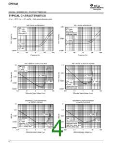
FREQUENCY RESPONSE
Small-Signal Bandwidth
66
dB
G = +1, R = 348Ω
180
90
MHz
MHz
MHz
MHz
MHz
dB
F
(V = 100mV , Peaking < 0.5 dB)
PP
G = +2, R = 602Ω
O
F
G = +5, R = 1.5kΩ
36
F
G = +10, R = 3.01kΩ
18
F
Bandwidth for 0.1dB Flatness
Peaking at a Gain of 1
Large-Signal Bandwidth
Slew Rate (25% to 75% )
Rise and Fall Time
G = +1, V = 100mV
40
O
PP
V
= 100mV
0.5
800
50
O
PP
G = +2, V = 20V
kHz
V/µs
ns
O
PP
G = +1
G = +1, V = 5V Step
100
75
O
Settling Time to 0.1%
G = +1, V = 2V Step
ns
O
0.01%
G = +1, V = 2V Step
200
ns
O
Total Harmonic Distortion + Noise
Differential Input/Output
Differential Input/Output
Single-Ended In/Differential Out
Single-Ended In/Differential Out
Intermodulation Distortion
Differential Input/Output
Differential Input/Output
Single-Ended In/Differential Out
Single-Ended In/Differential Out
Headroom
G = +1, f = 1kHz, V = 3Vrms
O
R
= 600Ω
0.0003
%
%
%
%
L
R
= 2kΩ
0.000022
0.000059
0.000043
L
R
= 600Ω
L
R
= 2kΩ
L
G = +1, SMPTE/DIN, V = 2V
O
PP
R
= 600Ω
0.00008
0.00005
0.0001
0.0007
20.0
%
%
%
%
L
L
R
= 2kΩ
L
R
= 600Ω
R
= 2kΩ
L
THD < 0.01%, R = 2kΩ
V
PP
L
OUTPUT
Voltage Output Swing
R
= 2kΩ
= 800Ω
(V+) − 1.9
(V+) − 4.5
+50/−60
(V−) + 1.9
(V−) + 4.5
V
V
L
R
L
Short-Circuit Current
I
Sourcing/Sinking
85
mA
SC
Closed-Loop Output Impedance
G = +1, f = 100kHz
0.3
Ω
(1)
POWER-DOWN
Enable Voltage Threshold
Disable Voltage Threshold
Shutdown Current
Turn-On Delay
(V−) + 2
V
V
(V−) + 0.8
V
= −15V
0.85
2
1.5
mA
µs
µs
ENABLE
Time for I to Reach 50%
Q
Turn-Off Delay
Time for I to Reach 50%
2
Q
POWER SUPPLY
Specified Operating Voltage
Operating Voltage
Quiescent Current
TEMPERATURE RANGE
Specified Range
15
14
16
V
V
2.5
I
Per Channel
17.1
mA
Q
−40
−40
−65
+85
+125
+150
_C
_C
Operating Range
Storage Range
_C
Thermal Resistance
200
_C/W
q
JA
(1)
Amplifier has internal 50kΩ pull-up resistor to V
CC+
pin. This enables the amplifier with no connection to shutdown pin.
3

 BB [ BURR-BROWN CORPORATION ]