ꢂ
ꢀ
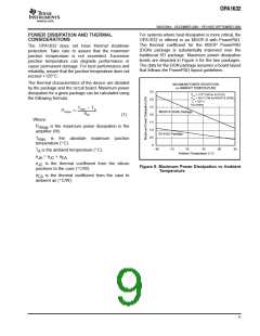
ꢉ
ꢠ
ꢡ
ꢢ
ꢣ
www.ti.com
SBOS286A − DECEMBER 2003 − REVISED SEPTEMBER 2006
(1)
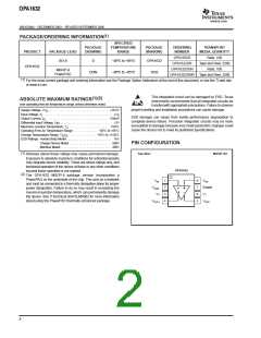
PACKAGE/ORDERING INFORMATION
SPECIFIED
TEMPERATURE
RANGE
PACKAGE
DRAWING
PACKAGE
MARKING
ORDERING
NUMBER
TRANSPORT
MEDIA, QUANTITY
PRODUCT
PACKAGE-LEAD
OPA1632D
OPA1632DR
OPA1632DGN
Rails, 100
Tape and Reel, 2500
Rails, 100
SO-8
D
−40°C to +85°C
−40°C to +85°C
OPA1632
1632
OPA1632
MSOP-8
PowerPAD
DGN
OPA1632DGNR Tape and Reel, 2500
(1)
For the most current package and ordering information see the Package Option Addendum at the end of this document, or see the TI web site
at www.ti.com.
This integrated circuit can be damaged by ESD. Texas
Instruments recommends that all integrated circuits be
handledwith appropriate precautions. Failure to observe
(1)(2)
ABSOLUTE MAXIMUM RATINGS
over operating free-air temperature range unless otherwise noted.
proper handling and installation procedures can cause damage.
Supply Voltage,
V . . . . . . . . . . . . . . . . . . . . . . . . . . . . . . . . . . . . . . . 16.5V
S
Input Voltage, V . . . . . . . . . . . . . . . . . . . . . . . . . . . . . . . . . . . . . . . . . . . . .
V
I
S
ESD damage can range from subtle performance degradation to
complete device failure. Precision integrated circuits may be more
susceptible to damage because very small parametric changes could
cause the device not to meet its published specifications.
Output Current, I . . . . . . . . . . . . . . . . . . . . . . . . . . . . . . . . . . . . . . . . 150mA
O
Differential Input Voltage, V
. . . . . . . . . . . . . . . . . . . . . . . . . . . . . . . . . . 3V
ID
Maximum Junction Temperature, T . . . . . . . . . . . . . . . . . . . . . . . . . . 150°C
J
Operating Free-Air Temperature Range . . . . . . . . . . . . . . . −40°C to +85°C
Storage Temperature Range, T
. . . . . . . . . . . . . . . . . −65°C to +150°C
STG
ESD Ratings: Human Body Model . . . . . . . . . . . . . . . . . . . . . . . . . . . . . . 1kV
Charge Device Model . . . . . . . . . . . . . . . . . . . . . . . . . . . 500V
Machine Model . . . . . . . . . . . . . . . . . . . . . . . . . . . . . . . . . 200V
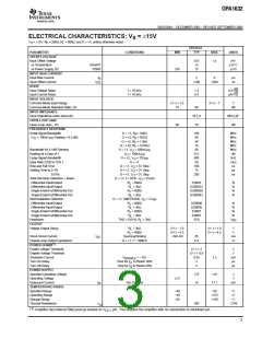
PIN CONFIGURATION
(1)
Top View
MSOP, SO
Stresses above these ratings may cause permanent damage.
Exposure to absolute maximum conditions for extended periods
may degrade device reliability. These are stress ratings only, and
functional operation of the device at these or any other conditions
beyond those specified is not implied.
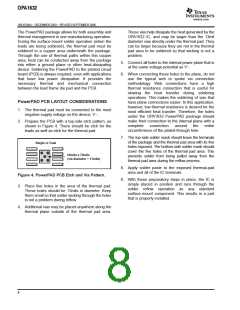
The OPA1632 MSOP-8 package version incorporates a
PowerPAD on the underside of the chip. This acts as a heatsink
and must be connected to a thermally dissipative plane for proper
power dissipation. Failure to do so may result in exceeding the
maximumjunction temperature, which can permanently damage
the device. See TI technical brief SLMA002 for more information
about using the PowerPAD thermally enhanced package.
OPA1632
(2)
VIN+
VIN
1
2
3
4
8
7
6
5
−
VOCM
V+
Enable
−
V
VOUT+
VOUT−
2

 BB [ BURR-BROWN CORPORATION ]