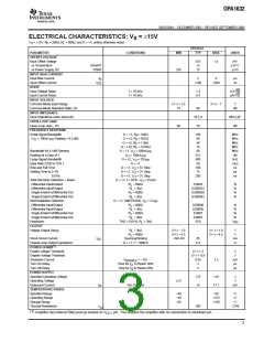
ꢂ ꢀꢉ ꢠꢡꢢ ꢣ
www.ti.com
SBOS286A − DECEMBER 2003 − REVISED SEPTEMBER 2006
Quiescent current is reduced to approximately 0.85mA
when the amplifier is disabled. When disabled, the
output stage is not in a high-impedance state. Thus, the
shutdown function cannot be used to create a
multiplexed switching function in series with multiple
amplifiers.
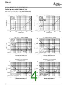
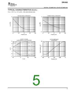
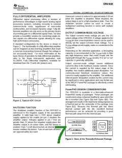
FULLY-DIFFERENTIAL AMPLIFIERS
Differential signal processing offers a number of
performance advantages in high-speed analog signal
processing systems, including immunity to external
common-mode noise, suppression of even-order
nonlinearities, and increased dynamic range. Fully-dif-
ferential amplifiers not only serve as the primary means
of providing gain to a differential signal chain, but also
provide a monolithic solution for converting single-en-
ded signals into differential signals allowing for easy,
high-performance processing.
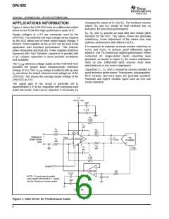
OUTPUT COMMON-MODE VOLTAGE
The output common-mode voltage pin sets the DC
output voltage of the OPA1632. A voltage applied to the
V
pin from a low-impedance source can be used to
OCM
directly set the output common-mode voltage. For a
A standard configuration for the device is shown in
Figure 2. The functionality of a fully differential amplifier
can be imagined as two inverting amplifiers that share
a common noninverting terminal (though the voltage is
not necessarily fixed). For more information on the
basic theory of operation for fully differential amplifiers,
refer to the Texas Instruments application note
SLOA054, Fully Differential Amplifiers, available for
download from the TI web site (www.ti.com).
V
V
voltage at mid-supply, make no connection to the
pin.
OCM
OCM
Depending on the intended application, a decoupling
capacitor is recommended on the V node to filter
any high-frequency noise that could couple into the
signal path through the V
OCM
circuitry. A 0.1µF or 1µF
OCM
capacitor is generally adequate.
Output common-mode voltage causes additional
current to flow in the feedback resistor network. Since
this current is supplied by the output stage of the
amplifier, this creates additional power dissipation. For
commonly-used feedback resistance values, this
current is easily supplied by the amplifier. The additional
internal power dissipation created by this current may
be significant in some applications and may dictate use
of the MSOP PowerPAD package to effectively control
self-heating.
+15V
Digital
Output
VIN+
AIN
VOCM
VIN
AIN
−
VREF
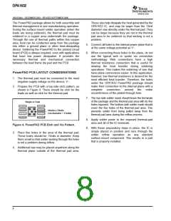
PowerPAD DESIGN CONSIDERATIONS
−
15V
The OPA1632 is available in a thermally-enhanced
PowerPAD family of packages. These packages are
constructed using a downset leadframe upon which the
die is mounted (see Figure 3[a] and Figure 3[b]). This
arrangement results in the lead frame being exposed as
a thermal pad on the underside of the package (see
Figure 3[c]). Because this thermal pad has direct
thermal contact with the die, excellent thermal
performance can be achieved by providing a good
thermal path away from the thermal pad.
Figure 2. Typical ADC Circuit
SHUTDOWN FUNCTION
The shutdown (enable) function of the OPA1632 is
referenced to the negative supply of the operational
amplifier. A valid logic low (< 0.8V above negative
supply) applied to the enable pin (pin 7) disables the
amplifier output. Voltages applied to pin 7 that are
greater than 2V above the negative supply place the
amplifier output in an active state, and the device is
enabled. If pin 7 is left disconnected, an internal pull-up
resistor enables the device. Turn-on and turn-off times
are approximately 2µs each.
DIE
Thermal
Pad
(a) Side View
DIE
(b) End View
(c) Bottom View
Figure 3. Views of the Thermally-Enhanced Package.
7

 BB [ BURR-BROWN CORPORATION ]