ꢂꢀꢉꢠ ꢡꢢ ꢣ
www.ti.com
SBOS286A − DECEMBER 2003 − REVISED SEPTEMBER 2006
The PowerPAD package allows for both assembly and
thermal management in one manufacturing operation.
During the surface-mount solder operation (when the
leads are being soldered), the thermal pad must be
soldered to a copper area underneath the package.
Through the use of thermal paths within this copper
area, heat can be conducted away from the package
into either a ground plane or other heat-dissipating
device. Soldering the PowerPAD to the printed circuit
board (PCB) is always required, even with applications
that have low power dissipation. It provides the
necessary thermal and mechanical connection
between the lead frame die pad and the PCB.
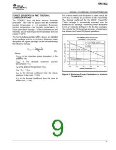
These vias help dissipate the heat generated by the
OPA1632 IC, and may be larger than the 13mil
diameter vias directly under the thermal pad. They
can be larger because they are not in the thermal
pad area to be soldered so that wicking is not a
problem.
5. Connect all holes to the internal power plane that is
at the same voltage potential as V−.
6. When connecting these holes to the plane, do not
use the typical web or spoke via connection
methodology. Web connections have a high
thermal resistance connection that is useful for
slowing the heat transfer during soldering
operations. This makes the soldering of vias that
have plane connections easier. In this application,
however, low thermal resistance is desired for the
most efficient heat transfer. Therefore, the holes
under the OPA1632 PowerPAD package should
make their connection to the internal plane with a
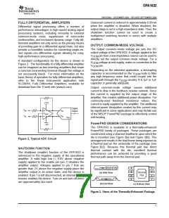
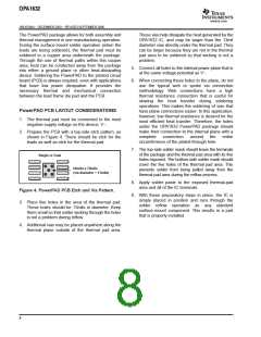
PowerPAD PCB LAYOUT CONSIDERATIONS
1. The thermal pad must be connected to the most
negative supply voltage on the device, V−.
2. Prepare the PCB with a top-side etch pattern, as
shown in Figure 4. There should be etch for the
leads as well as etch for the thermal pad.
complete
connection
around
the
entire
circumference of the plated-through hole.
7. The top-side solder mask should leave the terminals
of the package and the thermal pad area with its five
holes exposed. The bottom-side solder mask should
cover the five holes of the thermal pad area. This
prevents solder from being pulled away from the
thermal pad area during the reflow process.
Single or Dual
68mils x 70mils
(via diameter = 13mils)
8. Apply solder paste to the exposed thermal-pad
area and all of the IC terminals.
Figure 4. PowerPAD PCB Etch and Via Pattern.
9. With these preparatory steps in place, the IC is
simply placed in position and runs through the
solder reflow operation as any standard
surface-mount component. This results in a part
that is properly installed.
3. Place five holes in the area of the thermal pad.
These holes should be 13mils in diameter. Keep
them small so that solder wicking through the holes
is not a problem during reflow.
4. Additional vias may be placed anywhere along the
thermal plane outside of the thermal pad area.
8

 BB [ BURR-BROWN CORPORATION ]