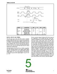
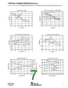
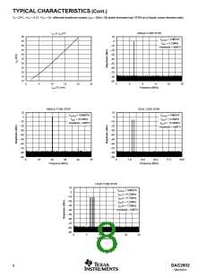
TIMING DIAGRAM
tS
tH
DATA IN
D[11:0](n)
D[11:0](n + 1)
tLPW
WRT1
WRT2
tCPW
CLK1
CLK2
tCW
tSET
IOUT
1
IOUT(n)
IOUT(n +1)
50%
I
OUT2
tPD
SYMBOL
DESCRIPTION
MIN
TYP
MAX
UNITS
tS
tH
Input Setup Time
Input Hold Time
Latch/Clock Pulsewidth
Delay Rising CLK Edge to
Rising WRT Edge
2
1.5
3.5
0
ns
ns
ns
ns
t
LPW, tCPW
4
tCW
tPW – 2
tPD
tSET
Propagation Delay
Settling Time (0.1%)
1
30
ns
ns
DIGITAL INPUTS AND TIMING
The two converter channels within the DAC2902 consist of
two independent, 12-bit, parallel data ports. Each DAC-
channel is controlled by its own set of write (WRT1, WRT2)
and clock (CLK1, CLK2) inputs. Here, the WRT lines
control the channel input latches and the CLK lines control
the DAC latches. The data is first loaded into the input latch
by a rising edge of the WRT line. This data is presented to
the DAC latch on the following falling edge of the WRT
signal. On the next rising edge of the CLK line, the DAC is
updated with the new data and the analog output signal will
change accordingly. The double latch architecture of the
DAC2902 results in a defined sequence for the WRT and
CLK signals, expressed by parameter ‘tCW’. A correct tim-
ing is observed when the rising edge of CLK occurs at the
same time, or before, the rising edge of the WRT signal. This
condition can simply be met by connecting the WRT and
CLK lines together. Note that all specifications were mea-
sured with the WRT and CLK lines connected together.
The data input ports of the DAC2902 accepts a standard
positive coding with data bit D11 being the most significant
bit (MSB). The converter outputs support a clock rate of up
to 125MSPS. The best performance will typically be achieved
with a symmetric duty cycle for write and clock; however,
the duty cycle may vary as long as the timing specifications
are met. Also, the set-up and hold times may be chosen
within their specified limits.
All digital inputs of the DAC2902 are CMOS compatible.
The logic thresholds depend on the applied digital supply
voltages, such that they are set to approximately half the
supply voltage; Vth = +VD/2 (±20% tolerance). The DAC2902
is designed to operate with a digital supply (+VD) of +3.0V
to +5.5V.
DAC2902
SBAS167A
5

 BB [ BURR-BROWN CORPORATION ]