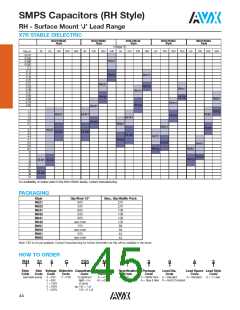
SMPS Capacitors
Assembly Guidelines
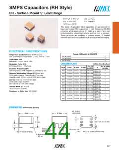
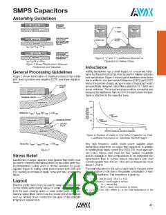
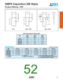
DIMENSIONS
AT AMBIENT
TEMPERATURE
CAPACITOR
CAPACITOR
"J" LEADS
"L" LEADS
CAPACITOR
BODY
CAPACITOR
BODY
SUBSTRATE
SUBSTRATE LINEAR
DISPLACEMENT
PUTS SOLDER JOINT
AND CAPACITOR IN
TENSION
SOLDER
FILLETS
CAPACITOR
SUBSTRATE
SOLDER LAND
T
> T
CTE
> CTE
sub cap
oper
amb
SUBSTRATE
SUBSTRATE LINEAR
DISPLACEMENT
PUTS SOLDER JOINT
AND CAPACITOR IN
COMPRESSION
CAPACITOR
SUBSTRATE
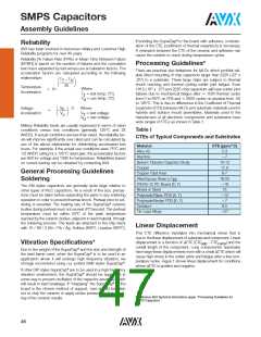
Figure 3. “J” and “L” Leadframes Mounted on
Capacitors to Relieve Stress
T
> T
CTE
< CTE
sub cap
oper
amb
Figure 1. Linear Displacement Between
Component and Substrate
Inductance
Adding leadframes has a small impact on component induc-
tance but this is the price that must be paid for reliable operation
over temperature. Figure 4 shows typical leadframe inductance
that is added for two lead standoff distances (0.020" and 0.050")
General Processing Guidelines
Figure 2 shows the location of maximum stress in the solder
joint due to positive and negative DCTE and linear displace-
ment.
®
versus the number of leads along one side of SupraCap which
SOLDER
FILLET
are specifically designed output filter capacitors for 1 MHz and
above switchers. The actual inductance will be somewhat less
because the leadframes flare out from the lead where the lead-
frame is attached to the capacitor body.
CAPACITOR
MAXIMUM STRESS
SUBSTRATE
0.4
0.3
Stress for T
> T
CTE
> CTE
sub cap
oper
amb
0.2
0.050"
Standoff
0.020"
0.1
MAXIMUM STRESS
CAPACITOR
Standoff
SOLDER
FILLET
0
5
10
15
20
Number of leads on one side of Capacitor
SUBSTRATE
Figure 4. Number of Leads on One Side of Capacitor vs. Total
Leadframe Inductance vs. Substrate Standoff Height
Stress for T
> T
CTE
< CTE
sub cap
Very high frequency switch mode power supplies place
tremendous restrictions on output filter capacitors. In addition
to handling high ripple current (low ESR), ESL must approach
zero nano henrys, part must be truly surface mountable
and be available in new configurations to be integrated into
transmission lines to further reduce inductance with load
currents greater than 40A at 1 MHz and as frequencies move
above 1-2 MHz.
oper
amb
Figure 2
Stress Relief
Leadframes on larger capacitor sizes (greater than 2225) must
be used to minimize mechanical stress on the solder joints dur-
ing temperature cycling which is normal operation for power
supplies (Figure 3). Failing solder joints increase both ESR and
ESL causing an increase in ripple, noise and heat, accelerating
failure.
The total inductance is the sum of each side of the part where
the inductance of one side is the parallel combination of each
lead in the leadframe. That inductance is given by:
L (nH) = 5xꢀ [In (2xꢀ) / (B+C) + 1/2]
Where ꢀ = lead length in inches
Layout
In = natural log
Effective solder dams must be used to keep all molten solder
on the solder lands during reflow or solder will migrate away
from the land, causing opens or weak solder joints. High fre-
quency output filters cannot use low power layout techniques
such as necked down conductors because of the stringent
inductance requirements.
B+C = lead cross section in inches
so L (nH) = 2xL (nH) where L is the total inductance of the
1
1
leadframe.
47

 KYOCERA AVX [ KYOCERA AVX ]