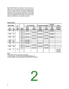
HCPL-2602,HCPL-2612
HighCMRLineReceiverOptocouplers
DataSheet
Description
Features
TheHCPL-2602/12areopticallycoupledlinereceivers
that combine a GaAsP light emitting diode, an input
current regulator and an integrated high gain photo
detector. The input regulator serves as a line
termination for line receiver applications. It clamps
the line voltage and regulates the LED current so line
reflections do not interfere with circuit performance.
• 1000 V/ µs minimum Common Mode Rejection (CMR) at
VCM = 50 V for HCPL-2602 and 3.5 kV/ µs minimum
CMR at VCM = 300 V for HCPL-2612
• Line termination included – no extra circuitry required
• Accepts a broad range of drive conditions
• LED protection minimizes LED efficiency degradation
• High speed: 10 MBd (limited by transmission line in
many applications)
The regulator allows a typical LED current of 8.5 mA
before it starts to shunt excess current. The output
ofthedetectorICisanopencollectorSchottkyclamped
• Guaranteed AC and DC performance over temperature:
0°C to 70°C
transistor. An enable input gates the detector. The • External base lead allows “LED peaking” and LED
internal detector shield provides a guaranteed
common mode transient immunity specification of
1000 V/ms for the 2602, and 3500 V/ms for the 2612.
current adjustment
• Safety approval
UL recognized – 3750 V rms for 1 Minute
CSA approved
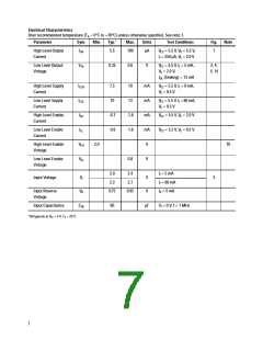
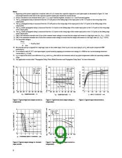
DC specifications are defined similar to TTL logic.
The optocoupler ac and dc operational parameters
are guaranteed from 0°C to 70°C allowing trouble-
free interfacing with digital logic circuits. An input
current of 5 mA will sink an eight gate fan-out (TTL)
at the output.
• MIL-PRF-38534 hermetic version available (HCPL-1930/ 1)
Applications
• Isolated line receiver
• Computer-peripheral interface
• Microprocessor system interface
• Digital isolation for A/ D, D/ A conversion
• Current sensing
• Instrument input/ output isolation
• Ground loop elimination
• Pulse transformer replacement
• Power transistor isolation in motor drives
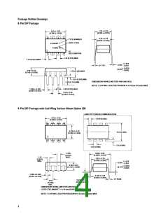
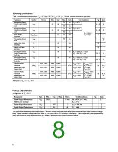
Functional Diagram
TRUTH TABLE
(POSITIVE LOGIC)
V
1
2
8
7
NC
IN+
CC
LED ENABLE OUTPUT
ON
OFF
ON
OFF
ON
OFF
H
H
L
L
NC
NC
L
H
H
H
L
V
E
V
IN–
3
4
6
5
O
GND
CATHODE
H
SHIELD
A 0.1 µF bypass capacitor must be connected between pins 5 and 8.
CAUTION: It is advised that normal static precautions be taken in handling and assembly of this component to
prevent damage and/or degradation which may be induced by ESD.

 AVAGO [ AVAGO TECHNOLOGIES LIMITED ]