VRAM
SMJ44C251B
MT42C4256
Austin Semiconductor, Inc.
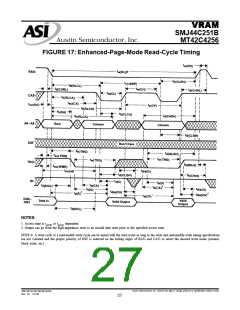
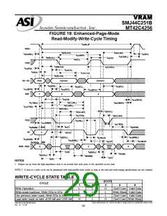
FIGURE 19: Enhanced-Page-Mode
Read-Modify-Write-Cycle Timing
NOTES:
1. Output can go from the high-impedance state to an invalid data state prior to the specified access time.
NOTE C: A read or a write cycle can be intermixed with read-modify-write cycles as long as the read and write timing specifications are not violated.
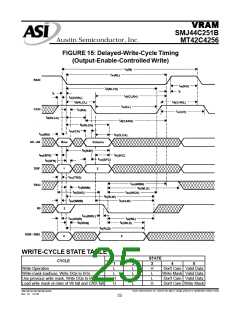
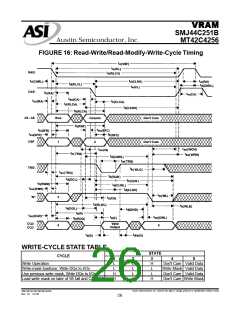
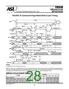
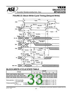
WRITE-CYCLE STATE TABLE
STATE
CYCLE
1
L
L
H
H
2
L
L
L
L
3
H
L
L
H
4
5
Write Operation
Don't Care Valid Data
Write Mask Valid Data
Don't Care Valid Data
Don't Care Write Mask
Write-mask load/use, Write DQs to I/Os
Use previous write mask, Write DQs to I/Os
Load write mask on later of W\ fall and CAS\ fall
Austin Semiconductor, Inc. reserves the right to change products or specifications without notice.
SMJ44C251B/MT42C4256
Rev. 0.1 12/03
29

 AUSTIN [ AUSTIN SEMICONDUCTOR ]