VRAM
SMJ44C251B
MT42C4256
Austin Semiconductor, Inc.
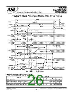
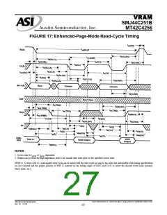
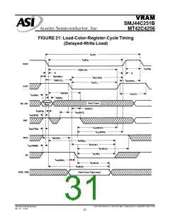
FIGURE 17: Enhanced-Page-Mode Read-Cycle Timing
NOTES:
1. Access time is ta(CP) or ta(CA) dependent.
2. Output can go from the high-impedance state to an invalid data state prior to the specified access time.
NOTE A: A write cycle or a read-modify-write cycle can be mixed with the read cycles as long as the write and read-modify-write timing specifications
are not violated and the proper polarity of DSF is selected on the falling edges of RAS\ and CAS\ to select the desired write mode (normal,
block write, etc.)
Austin Semiconductor, Inc. reserves the right to change products or specifications without notice.
SMJ44C251B/MT42C4256
Rev. 0.1 12/03
27

 AUSTIN [ AUSTIN SEMICONDUCTOR ]