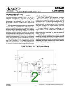
SDRAM
AS4SD8M16
Austin Semiconductor, Inc.
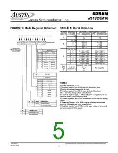
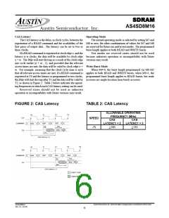
CAS Latency
The CAS latency is the delay, in clock cycles, between the
Operating Mode
The normal operating mode is selected by setting M7 and
registration of a READ command and the availability of the M8 to zero; the other combinations of values for M7 and M8
first piece of output data. The latency can be set to two or are reserved for future use and/or test modes. The programmed
three clocks.
If a READ command is registered at clock edge n, and the
burst length applies to both READ and WRITE bursts.
Test modes are reserved states should not be used
latency is m clocks, the data will be available by clock edge because unknown operation or incompatibility with future
n + m. The DQs will start driving as a result of the clock edge versions may result.
one cycle earlier (n + m - 1), and provided that the relevant
access times are met, the data will be valid by clock edge n + Write Burst Mode
m. For example, assuming that the clock cycle time is such
When M9=0, the burst length programmed via M0-M2
that all relevant access times are met, if a READ command is applies to both READ and WRITE bursts; when M9=1, the
registered at T0 and the latency is programmed to two clocks, programmed burst length applies to READ bursts, but write
the DQs will start driving after T1 and the data will be valid by accesses are single-location (non-burst) accesses.
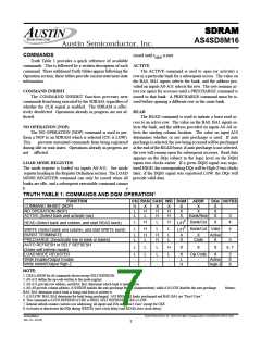
T2, as shown in Figure 2. Table 2 below indicates the operat-
ing frequencies at which each CAS latency setting can be used.
Reserved states should not be used as unknown
operation or incompatibility with future versions may result.
FIGURE 2: CAS Latency
TABLE 2: CAS Latency
ALLOWABLE OPERATING
FREQUENCY (MHz)
SPEED
CAS
LATENCY = 2
<100
CAS
LATENCY = 3
<133
-75
Austin Semiconductor, Inc. reserves the right to change products or specifications without notice.
AS4SD8M16
Rev. 0.5 04/05
6

 AUSTIN [ AUSTIN SEMICONDUCTOR ]