SDRAM
AS4SD8M16
Austin Semiconductor, Inc.
issued until tMRD is met.
COMMANDS
Truth Table 1 provides a quick reference of available
ACTIVE
commands. This is followed by a written description of each
command. Three additional Truth Tables appear following the
Operation section; these tables provide current state/next state
information.
The ACTIVE command is used to open (or activate) a
row in a particular bank for a subsequent access. The value on
the BA0, BA1 inputs selects the bank, and the address pro-
vided on inputs A0-A11 selects the row. The row remains ac-
tive (or open) for accesses until a PRECHARGE command is
issued to that bank. A PRECHARGE command must be is-
sued before opening a different row in the same bank.
COMMAND INHIBIT
The COMMAND INHIBIT function prevents new
commands from being executed by the SDRAM, regardless of
whether the CLK signal is enabled. The SDRAM is effec-
tively deselected. Operations already in progress are not af-
fected.
READ
The READ command is used to initiate a burst read ac-
cess to an active row. The value on the BA0, BA1 inputs se-
lects the bank, and the address provided on inputs A0-A8 se-
lects the starting column location. The value on input A10
determines whether or not auto precharge is used. If auto
precharge is selected, the row being accessed will be precharged
at the end of the READ burst; if auto precharge is not selected,
the row will remain open for subsequent accesses. Read data
appears on the DQs subject to the logic level on the DQM
inputs two clocks earlier. If a given DQM signal was regis-
tered HIGH, the corresponding DQs will be High-Z two clocks
later; if the DQM signal was registered LOW, the DQs will
provide valid data.
NO OPERATION (NOP)
The NO OPERATION (NOP) command is used to per-
form a NOP to an SDRAM which is selected (CS\ is LOW).
This
prevents unwanted commands from being registered
during idle or wait states. Operations already in progress are
not affected.
LOAD MODE REGISTER
The mode register is loaded via inputs A0-A11. See mode
register heading in the Register Definition section. The LOAD
MODE REGISTER command can only be issued when all
banks are idle, and a subsequent executable command cannot
b
e
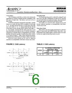
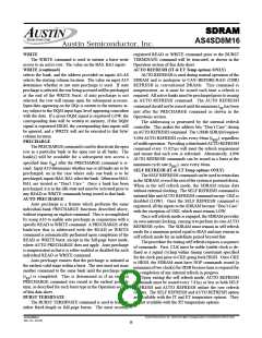
TRUTH TABLE 1: COMMANDS AND DQM OPERATION1
FUNCTION
COMMAND INHIBIT (NOP)
NO OPERATION (NOP)
CS\ RAS\ CAS\ WE\ DQM
ADDR
DQs NOTES
X
X
H
L
L
X
H
L
X
H
H
X
H
H
X
X
X
X
X
ACTIVE (Select bank and activate row)
Bank/Row
X
3
4
8
8
L
L
H
H
L
L
H
L
Bank/Col
X
L/H
READ (Select bank and column, and start READ burst)
Bank/Col Valid
4
L/H
X
X
WRITE (Select bank and column, and start WRITE burst)
BURST TERMINATE
PRECHARGE (Deactivate row in bank or banks)
AUTO REFRESH or SELF REFRESH
(Enter self refresh mode)
L
L
H
L
H
H
L
L
X
Code
Active
X
5
L
L
L
H
X
X
X
6, 7
LOAD MODE REGISTER
Write Enable/Output Enable
Write Inhibit/Output High-Z
L
-
-
L
-
-
L
-
-
L
-
-
X
L
H
Op-Code
X
2
8
8
-
-
Active
High-Z
NOTE:
1. CKE is HIGH for all commands shown except SELF REFRESH.
2. A0-A11 define the op-code written to the mode register.
3. A0-A11 provide row address, and BA0, BA1 determine which bank is made active.
4. A0-A8 provide column address; A10 HIGH enables the auto precharge feature (nonpersistent), while A10 LOW disables the auto precharge
BA0, BA1 determine which bank is being read from or written to.
feature;
5. A10 LOW: BA0, BA1 determine the bank being precharged. A10 HIGH: All banks precharged and BA0, BA1 are “Don’t Care.”
6. This command is AUTO REFRESH if CKE is HIGH, SELF REFRESH if CKE is LOW.
7. Internal refresh counter controls row addressing; all inputs and I/Os are “Don’t Care” except for CKE.
8. Activates or deactivates the DQs during WRITEs (zero-clock delay) and READs (two-clock delay).
Austin Semiconductor, Inc. reserves the right to change products or specifications without notice.
AS4SD8M16
Rev. 0.5 04/05
7

 AUSTIN [ AUSTIN SEMICONDUCTOR ]