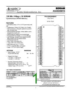
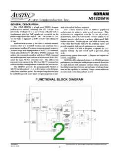
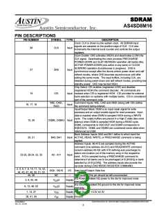
SDRAM
AS4SD8M16
Austin Semiconductor, Inc.
GENERAL DESCRIPTION
The 128Mb SDRAM is a high-speed CMOS, dynamic
random-access memory containing 134, 217, 728 bits. It is
internally configured as a quad-bank DRAM with a
synchronous interface (all signals are registered on the
positive edge of the clock signal, CLK). Each of the 33, 554,
432-bit banks is organized as 4,096 rows by 512 columns by
16 bits.
Read and write accesses to the SDRAM are burst oriented;
accesses start at a selected location and continue for a
programmed number of locations in a programmed sequence.
Accesses begin with the registration of anACTIVE command,
which is then followed by a READ or WRITE command. The
address bits registered coincident with the ACTIVE command
are used to select the bank and row to be accessed (BA0, BA1
select the bank; A0-A11 select the row). The address bits
registered coincident with the READ or WRITE command are
used to select the starting column location for the burst access.
The SDRAM provides for programmable READ or
WRITE burst lengths of 1, 2, 4, or 8 locations, or the full page,
with a burst terminate option. An auto precharge function may
be enabled to provide a self-timed row precharge that is initi-
ated at the end of the burst sequence.
The 128Mb SDRAM uses an internal pipelined
architecture to achieve high-speed operation. This
architecture is compatible with the 2n rule of prefetch
architectures, but it also allows the column address to be
changed on every clock cycle to achieve a high-speed, fully
random operation. Precharging one bank while accessing one
of the other three banks will hide the precharge cycles and
provide seamless, high-speed, random-access operation.
The 128Mb SDRAM is designed to operate in 3.3V
memory systems. An auto refresh mode is provided, along
with
a
power-saving, power-down mode. All inputs and outputs are
LVTTL-compatible.
SDRAMs offer substantial advances in DRAM operating
performance, including the ability to synchronously burst data
at a high data rate with automatic column-address generation,
the ability to interleave between internal banks to hide precharge
time and the capability to randomly change column addresses
on each clock cycle during a burst access.
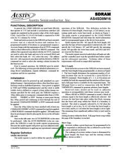
FUNCTIONAL BLOCK DIAGRAM
Austin Semiconductor, Inc. reserves the right to change products or specifications without notice.
AS4SD8M16
Rev. 0.5 04/05
2

 AUSTIN [ AUSTIN SEMICONDUCTOR ]