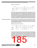
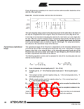
AT90CAN128
USART Register
Description
USART0 I/O Data Register –
UDR0
Bit
7
6
5
4
3
2
1
0
RXB0[7:0]
TXB0[7:0]
UDR0 (Read)
UDR0 (Write)
Read/Write
Initial Value
R/W
0
R/W
0
R/W
0
R/W
R/W
0
R/W
0
R/W
0
R/W
0
0
USART1 I/O Data Register –
UDR1
Bit
7
6
5
4
3
2
1
0
RXB1[7:0]
TXB1[7:0]
UDR1 (Read)
UDR1 (Write)
Read/Write
Initial Value
R/W
0
R/W
0
R/W
0
R/W
R/W
0
R/W
0
R/W
0
R/W
0
0
• Bit 7:0 – RxBn7:0: Receive Data Buffer (read access)
• Bit 7:0 – TxBn7:0: Transmit Data Buffer (write access)
The USARTn Transmit Data Buffer Register and USARTn Receive Data Buffer Regis-
ters share the same I/O address referred to as USARTn Data Register or UDRn. The
Transmit Data Buffer Register (TXBn) will be the destination for data written to the
UDRn Register location. Reading the UDRn Register location will return the contents of
the Receive Data Buffer Register (RXBn).
For 5-, 6-, or 7-bit characters the upper unused bits will be ignored by the Transmitter
and set to zero by the Receiver.
The transmit buffer can only be written when the UDREn flag in the UCSRnA Register is
set. Data written to UDRn when the UDREn flag is not set, will be ignored by the
USARTn Transmitter. When data is written to the transmit buffer, and the Transmitter is
enabled, the Transmitter will load the data into the Transmit Shift Register when the
Shift Register is empty. Then the data will be serially transmitted on the TxDn pin.
The receive buffer consists of a two level FIFO. The FIFO will change its state whenever
the receive buffer is accessed.
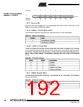
USART0 Control and Status
Register A – UCSR0A
Bit
7
RXC0
R
6
5
UDRE0
R
4
FE0
R
3
DOR0
R
2
UPE0
R
1
0
TXC0
R/W
U2X0
R/W
MPCM0
R/W
UCSR0A
UCSR1A
Read/Write
Initial Value
0
0
1
0
0
0
0
0
USART1 Control and Status
Register A – UCSR1A
Bit
7
RXC1
R
6
5
UDRE1
R
4
FE1
R
3
DOR1
R
2
UPE1
R
1
0
TXC1
R/W
U2X1
R/W
MPCM1
R/W
Read/Write
Initial Value
0
0
1
0
0
0
0
0
• Bit 7 – RXCn: USARTn Receive Complete
This flag bit is set when there are unread data in the receive buffer and cleared when the
receive buffer is empty (i.e., does not contain any unread data). If the Receiver is dis-
abled, the receive buffer will be flushed and consequently the RXCn bit will become
zero. The RXCn flag can be used to generate a Receive Complete interrupt (see
description of the RXCIEn bit).
189
4250E–CAN–12/04

 ATMEL [ ATMEL ]