AT90CAN128
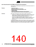
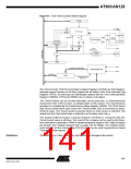
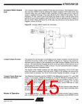
Figure 61. 8-bit Timer/Counter2 Block Diagram
TCCRnx
count
TOVn
(Int.Req.)
clear
Control Logic
direction
clkTn
TOSC2
T/C
BOTTOM
TOP
Oscillator
Prescaler
TOSC1
Timer/Counter
TCNTn
= 0
= 0xFF
clkI/O
OCnx
(Int.Req.)
Waveform
Generation
OCnx
=
OCRnx
clkI/O
Synchronized Status flags
Synchronization Unit
clkASY
Status flags
ASSRn
asynchronous mode
select (ASn)
The Timer/Counter (TCNT2) and Output Compare Register (OCR2A) are 8-bit registers.
Interrupt request (shorten as Int.Req.) signals are all visible in the Timer Interrupt Flag
Register (TIFR2). All interrupts are individually masked with the Timer Interrupt Mask
Register (TIMSK2). TIFR2 and TIMSK2 are not shown in the figure.
The Timer/Counter can be clocked internally, via the prescaler, or asynchronously
clocked from the TOSC1/2 pins, as detailed later in this section. The asynchronous
operation is controlled by the Asynchronous Status Register (ASSR). The Clock Select
logic block controls which clock source the Timer/Counter uses to increment (or decre-
ment) its value. The Timer/Counter is inactive when no clock source is selected. The
output from the Clock Select logic is referred to as the timer clock (clkT2).
The double buffered Output Compare Register (OCR2A) is compared with the
Timer/Counter value at all times. The result of the compare can be used by the Wave-
form Generator to generate a PWM or variable frequency output on the Output Compare
pin (OC2A). See “Output Compare Unit” on page 143 for details. The compare match
event will also set the compare flag (OCF2A) which can be used to generate an Output
Compare interrupt request.
Definitions
The definitions in Table 65 are also used extensively throughout the section.
141
4250E–CAN–12/04

 ATMEL [ ATMEL ]