AT90CAN128
by the CPU, regardless of whether clkT2 is present or not. A CPU write overrides (has
priority over) all counter clear or count operations.
The counting sequence is determined by the setting of the WGM21 and WGM20 bits
located in the Timer/Counter Control Register (TCCR2A). There are close connections
between how the counter behaves (counts) and how waveforms are generated on the
Output Compare output OC2A. For more details about advanced counting sequences
and waveform generation, see “Modes of Operation” on page 145.
The Timer/Counter Overflow Flag (TOV2) is set according to the mode of operation
selected by the WGM21:0 bits. TOV2 can be used for generating a CPU interrupt.
Output Compare Unit
The 8-bit comparator continuously compares TCNT2 with the Output Compare Register
(OCR2A). Whenever TCNT2 equals OCR2A, the comparator signals a match. A match
will set the Output Compare Flag (OCF2A) at the next timer clock cycle. If enabled
(OCIE2A = 1), the Output Compare Flag generates an Output Compare interrupt. The
OCF2A flag is automatically cleared when the interrupt is executed. Alternatively, the
OCF2A flag can be cleared by software by writing a logical one to its I/O bit location. The
Waveform Generator uses the match signal to generate an output according to operat-
ing mode set by the WGM21:0 bits and Compare Output mode (COM2A1:0) bits. The
max and bottom signals are used by the Waveform Generator for handling the special
cases of the extreme values in some modes of operation (“Modes of Operation” on page
145).
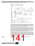
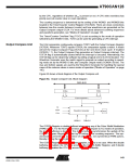
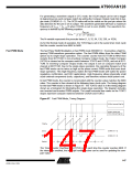
Figure 64 shows a block diagram of the Output Compare unit.
Figure 64. Output Compare Unit, Block Diagram
DATA BUS
OCRnx
TCNTn
= (8-bit Comparator )
OCFnx (Int.Req.)
top
bottom
FOCn
Waveform Generator
OCnx
WGMn1:0
COMnX1:0
The OCR2A Register is double buffered when using any of the Pulse Width Modulation
(PWM) modes. For the Normal and Clear Timer on Compare (CTC) modes of operation,
the double buffering is disabled. The double buffering synchronizes the update of the
OCR2A Compare Register to either top or bottom of the counting sequence. The syn-
chronization prevents the occurrence of odd-length, non-symmetrical PWM pulses,
thereby making the output glitch-free.
The OCR2A Register access may seem complex, but this is not case. When the double
buffering is enabled, the CPU has access to the OCR2A Buffer Register, and if double
buffering is disabled the CPU will access the OCR2A directly.
143
4250E–CAN–12/04

 ATMEL [ ATMEL ]