ATmega64A
hence, always consume power. In the deeper sleep modes, this will contribute significantly to
the total current consumption. Refer to “Brown-out Detector” on page 48 for details on how to
configure the Brown-out Detector.
9.7.4
Internal Voltage Reference
The internal voltage reference will be enabled when needed by the Brown-out Detector, the Ana-
log Comparator or the ADC. If these modules are disabled as described in the sections above,
the internal voltage reference will be disabled and it will not be consuming power. When turned
on again, the user must allow the reference to start up before the output is used. If the reference
is kept on in sleep mode, the output can be used immediately. Refer to “Internal Voltage Refer-
ence” on page 55 for details on the start-up time.
9.7.5
9.7.6
Watchdog Timer
If the Watchdog Timer is not needed in the application, this module should be turned off. If the
Watchdog Timer is enabled, it will be enabled in all sleep modes, and hence, always consume
power. In the deeper sleep modes, this will contribute significantly to the total current consump-
tion. Refer to “Watchdog Timer” on page 55 for details on how to configure the Watchdog Timer.
Port Pins
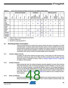
When entering a sleep mode, all port pins should be configured to use minimum power. The
most important thing is then to ensure that no pins drive resistive loads. In sleep modes where
the both the I/O clock (clkI/O) and the ADC clock (clkADC) are stopped, the input buffers of the
device will be disabled. This ensures that no power is consumed by the input logic when not
needed. In some cases, the input logic is needed for detecting wake-up conditions, and it will
then be enabled. Refer to the section “Digital Input Enable and Sleep Modes” on page 72 for
details on which pins are enabled. If the input buffer is enabled and the input signal is left floating
or have an analog signal level close to VCC/2, the input buffer will use excessive power.
9.7.7
JTAG Interface and On-chip Debug System
If the On-chip debug system is enabled by the OCDEN Fuse and the chip enter Power down or
Power save sleep mode, the main clock source remains enabled. In these sleep modes, this will
contribute significantly to the total current consumption. There are three alternative ways to
avoid this:
• Disable OCDEN Fuse.
• Disable JTAGEN Fuse.
• Write one to the JTD bit in MCUCSR.
The TDO pin is left floating when the JTAG interface is enabled while the JTAG TAP controller is
not shifting data. If the hardware connected to the TDO pin does not pull up the logic level,
power consumption will increase. Note that the TDI pin for the next device in the scan chain con-
tains a pull-up that avoids this problem. Writing the JTD bit in the MCUCSR register to one or
leaving the JTAG fuse unprogrammed disables the JTAG interface.
49
8160C–AVR–07/09

 ATMEL [ ATMEL ]