ATmega64A
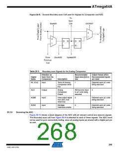
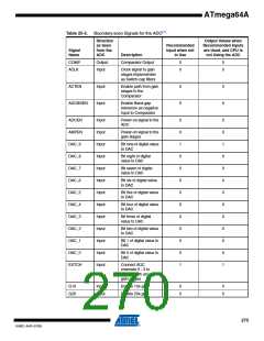
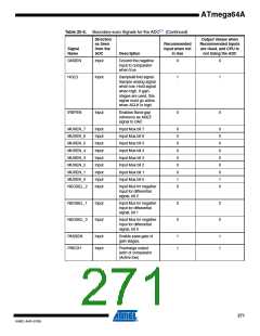
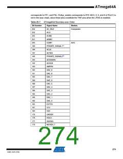
Table 25-5. Boundary-scan Signals for the ADC(1)
Direction
as Seen
from the
ADC
Output Values when
Recommended Inputs
are Used, and CPU is
not Using the ADC
Recommended
Input when not
in Use
Signal
Name
Description
COMP
ACLK
Output
Input
Comparator Output
0
0
0
0
Clock signal to gain
stages implemented
as Switch-cap filters
ACTEN
Input
Input
Enable path from gain
stages to the
Comparator
0
0
0
0
ADCBGEN
Enable Band-gap
reference as negative
input to Comparator
ADCEN
AMPEN
DAC_9
DAC_8
DAC_7
DAC_6
DAC_5
DAC_4
DAC_3
DAC_2
DAC_1
DAC_0
EXTCH
Input
Input
Input
Input
Input
Input
Input
Input
Input
Input
Input
Input
Input
Power-on signal to the
ADC
0
0
1
0
0
0
0
0
0
0
0
0
1
0
0
1
0
0
0
0
0
0
0
0
0
1
Power-on signal to the
gain stages
Bit nine of digital value
to DAC
Bit eight of digital
value to DAC
Bit seven of digital
value to DAC
Bit six of digital value
to DAC
Bit five of digital value
to DAC
Bit four of digital value
to DAC
Bit three of digital
value to DAC
Bit two of digital value
to DAC
Bit 1 of digital value to
DAC
Bit 0 of digital value to
DAC
Connect ADC
channels 0 - 3 to
bypass path around
gain stages
G10
G20
Input
Input
Enable 10x gain
Enable 20x gain
0
0
0
0
270
8160C–AVR–07/09

 ATMEL [ ATMEL ]