ATmega64A
As an example, consider the task of verifying a 1.5V 5% input signal at ADC channel 3 when
the power supply is 5.0V and AREF is externally connected to VCC
.
The lower limit is:
The upper limit is:
1024 ⋅ 1.5V ⋅ 0,95 ⁄ 5V = 291 = 0x123
1024 ⋅ 1.5V ⋅ 1.05 ⁄ 5V = 323 = 0x143
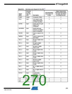
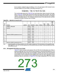
The recommended values from Table 25-5 are used unless other values are given in the algo-
rithm in Table 25-6. Only the DAC and Port Pin values of the Scan-chain are shown. The column
“Actions” describes what JTAG instruction to be used before filling the Boundary-scan Register
with the succeeding columns. The verification should be done on the data scanned out when
scanning in the data on the same row in the table.
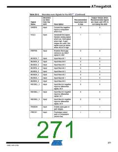
Table 25-6. Algorithm for Using the ADC(1)
PA3.
Pull-
Ste
p
PA3.
PA3.
up_
Enable
Actions
ADCEN
DAC
MUXEN HOLD PRECH Data Control
1
2
SAMPLE_PRELOAD
EXTEST
1
1
1
1
1
1
1
1
1
1
1
0x200
0x200
0x200
0x123
0x123
0x200
0x200
0x200
0x143
0x143
0x200
0x08
0x08
0x08
0x08
0x08
0x08
0x08
0x08
0x08
0x08
0x08
1
0
1
1
1
1
0
1
1
1
1
1
1
1
1
0
1
1
1
1
0
1
0
0
0
0
0
0
0
0
0
0
0
0
0
0
0
0
0
0
0
0
0
0
0
0
0
0
0
0
0
0
0
0
0
3
4
5
6
Verify the COMP bit scanned out to be 0
7
8
9
10
11
Note:
Verify the COMP bit scanned out to be 1
1. Using this algorithm, the timing constraint on the HOLD signal constrains the TCK clock frequency. As the algorithm keeps
HOLD high for five steps, the TCK clock frequency has to be at least five times the number of scan bits divided by the maxi-
mum hold time, thold,max
.
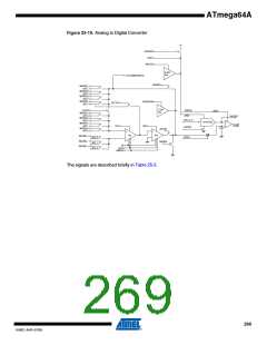
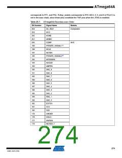
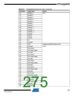
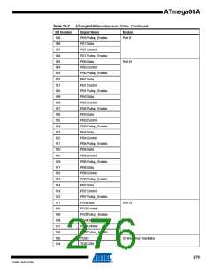
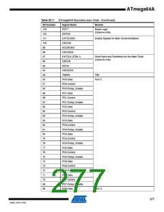
25.6 ATmega64A Boundary-scan Order
Table 25-7 shows the Scan order between TDI and TDO when the Boundary-scan Chain is
selected as data path. Bit 0 is the LSB; the first bit scanned in, and the first bit scanned out. The
scan order follows the pinout order as far as possible. Therefore, the bits of Port A are scanned
in the opposite bit order of the other ports. Exceptions from the rules are the scan chains for the
analog circuits, which constitute the most significant bits of the scan chain regardless of which
physical pin they are connected to. In Figure 25-3, PXn, Data corresponds to FF0, PXn. Control
273
8160C–AVR–07/09

 ATMEL [ ATMEL ]