ATmega64A
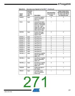
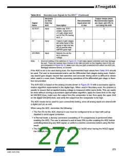
Table 25-5. Boundary-scan Signals for the ADC(1) (Continued)
Direction
Output Values when
Recommended Inputs
are Used, and CPU is
not Using the ADC
as Seen
from the
ADC
Recommended
Input when not
in Use
Signal
Name
Description
SCTEST
Input
Input
Input
Switch-cap TEST
enable. Output from
x10 gain stage send
out to Port Pin having
ADC_4
0
0
0
0
0
0
ST
Output of gain stages
will settle faster if this
signal is high first two
ACLK periods after
AMPEN goes high.
VCCREN
Selects Vcc as the
ACC reference
voltage.
Note:
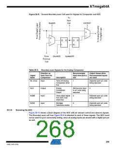
1. Incorrect setting of the switches in Figure 25-10 will make signal contention and may damage
the part. There are several input choices to the S&H circuitry on the negative input of the out-
put comparator in Figure 25-10. Make sure only one path is selected from either one ADC pin,
Bandgap reference source, or Ground.
If the ADC is not to be used during scan, the recommended input values from Table 25-5 should
be used. The user is recommended not to use the Differential Gain stages during scan. Switch-
cap based gain stages require fast operation and accurate timing which is difficult to obtain
when used in a scan chain. Details concerning operations of the differential gain stage is there-
fore not provided.
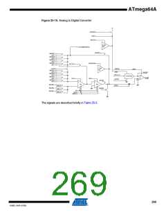
The AVR ADC is based on the analog circuitry shown in Figure 25-10 with a successive approx-
imation algorithm implemented in the digital logic. When used in Boundary-scan, the problem is
usually to ensure that an applied analog voltage is measured within some limits. This can easily
be done without running a successive approximation algorithm: apply the lower limit on the digi-
tal DAC[9:0] lines, make sure the output from the comparator is low, then apply the upper limit
on the digital DAC[9:0] lines, and verify the output from the comparator to be high.
The ADC needs not be used for pure connectivity testing, since all analog inputs are shared with
a digital port pin as well.
When using the ADC, remember the following:
• The Port Pin for the ADC channel in use must be configured to be an input with pull-up
disabled to avoid signal contention.
• In Normal mode, a dummy conversion (consisting of 10 comparisons) is performed when
enabling the ADC. The user is advised to wait at least 200 ns after enabling the ADC before
controlling/observing any ADC signal, or perform a dummy conversion before using the first
result.
• The DAC values must be stable at the midpoint value 0x200 when having the HOLD signal
low (Sample mode).
272
8160C–AVR–07/09

 ATMEL [ ATMEL ]