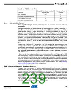
ATmega64A
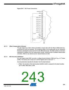
Figure 23-9. ADC Power Connections
(AD0) PA0 51
VCC
52
GND 53
(ADC7) PF7 54
(ADC6) PF6 55
(ADC5) PF5 56
(ADC4) PF4 57
(ADC3) PF3 58
(ADC2) PF2 59
(ADC1) PF1
(ADC0) PF0
60
61
10 μΗ
62
63
64
AREF
GND
AVCC
100 nF
1
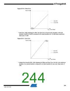
23.7.3
23.7.4
Offset Compensation Schemes
The gain stage has a built-in offset cancellation circuitry that nulls the offset of differential mea-
surements as much as possible. The remaining offset in the analog path can be measured
directly by selecting the same channel for both differential inputs. This offset residue can be then
subtracted in software from the measurement results. Using this kind of software based offset
correction, offset on any channel can be reduced below one LSB.
ADC Accuracy Definitions
An n-bit single-ended ADC converts a voltage linearly between GND and VREF in 2n steps
(LSBs). The lowest code is read as 0, and the highest code is read as 2n - 1.
Several parameters describe the deviation from the ideal behavior:
• Offset: The deviation of the first transition (0x000 to 0x001) compared to the ideal transition
(at 0.5 LSB). Ideal value: 0 LSB.
243
8160C–AVR–07/09

 ATMEL [ ATMEL ]