ATmega64A
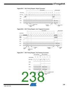
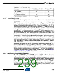
Table 23-1. ADC Conversion Time
Sample & Hold (Cycles from Start
of Conversion)
Conversion Time
(Cycles)
Condition
First conversion
13.5
1.5
25
13
Normal conversions, single ended
Auto Triggered conversions
Normal conversions, differential
2
13.5
13/14
1.5/2.5
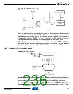
23.5.1
Differential Gain Channels
When using differential gain channels, certain aspects of the conversion need to be taken into
consideration.
Differential conversions are synchronized to the internal clock CKADC2 equal to half the ADC
clock. This synchronization is done automatically by the ADC interface in such a way that the
sample-and-hold occurs at a specific phase of CKADC2. A conversion initiated by the user (i.e., all
single conversions, and the first free running conversion) when CKADC2 is low will take the same
amount of time as a single ended conversion (13 ADC clock cycles from the next prescaled
clock cycle). A conversion initiated by the user when CKADC2 is high will take 14 ADC clock
cycles due to the synchronization mechanism. In Free Running mode, a new conversion is initi-
ated immediately after the previous conversion completes, and since CKADC2 is high at this time,
all automatically started (i.e., all but the first) free running conversions will take 14 ADC clock
cycles.
The gain stage is optimized for a bandwidth of 4 kHz at all gain settings. Higher frequencies may
be subjected to non-linear amplification. An external low-pass filter should be used if the input
signal contains higher frequency components than the gain stage bandwidth. Note that the ADC
clock frequency is independent of the gain stage bandwidth limitation. For example, the ADC
clock period may be 6 µs, allowing a channel to be sampled at 12 kSPS, regardless of the band-
width of this channel.
If differential gain channels are used and conversions are started by Auto Triggering, the ADC
must be switched off between conversions. When Auto Triggering is used, the ADC prescaler is
reset before the conversion is started. Since the gain stage is dependent of a stable ADC clock
prior to the conversion, this conversion will not be valid. By disabling and then re-enabling the
ADC between each conversion (writing ADEN in ADCSRA to “0” then to “1”), only extended con-
versions are performed. The result from the extended conversions will be valid. See “Prescaling
and Conversion Timing” on page 236 for timing details.
23.6 Changing Channel or Reference Selection
The MUXn and REFS1:0 bits in the ADMUX Register are single buffered through a temporary
register to which the CPU has random access. This ensures that the channels and reference
selection only takes place at a safe point during the conversion. The channel and reference
selection is continuously updated until a conversion is started. Once the conversion starts, the
channel and reference selection is locked to ensure a sufficient sampling time for the ADC. Con-
tinuous updating resumes in the last ADC clock cycle before the conversion completes (ADIF in
ADCSRA is set). Note that the conversion starts on the following rising ADC clock edge after
ADSC is written. The user is thus advised not to write new channel or reference selection values
to ADMUX until one ADC clock cycle after ADSC is written.
239
8160C–AVR–07/09

 ATMEL [ ATMEL ]