ATmega64A
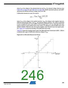
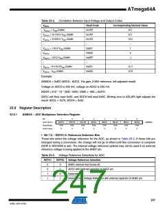
Table 23-2. Correlation Between Input Voltage and Output Codes
VADCn
Read Code
0x1FF
0x1FF
0x1FE
:.
Corresponding Decimal Value
VADCm + VREF/GAIN
511
511
510
:.
VADCm + 511/512 VREF/GAIN
VADCm + 510/512 VREF/GAIN
:.
V
ADCm + 1/512 VREF/GAIN
VADCm
ADCm - 1/512 VREF/GAIN
0x001
0x000
0x3FF
:.
1
0
V
-1
:.
:.
VADCm - 511/512VREF/GAIN
0x201
0x200
-511
-512
VADCm - VREF/GAIN
Example:
ADMUX = 0xED (ADC3 - ADC2, 10x gain, 2.56V reference, left adjusted result).
Voltage on ADC3 is 300 mV, voltage on ADC2 is 500 mV.
ADCR = 512 * 10 * (300 - 500) / 2560 = -400 = 0x270.
ADCL will thus read 0x00, and ADCH will read 0x9C. Writing zero to ADLAR right adjusts the
result: ADCL = 0x70, ADCH = 0x02.
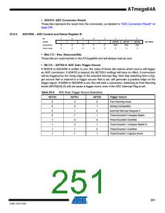
23.9 Register Description
23.9.1
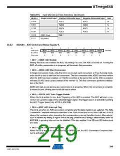
ADMUX – ADC Multiplexer Selection Register
Bit
7
REFS1
R/W
0
6
REFS0
R/W
0
5
ADLAR
R/W
0
4
MUX4
R/W
0
3
MUX3
R/W
0
2
MUX2
R/W
0
1
MUX1
R/W
0
0
MUX0
R/W
0
0x07 (0x27)
Read/Write
Initial Value
ADMUX
• Bit 7:6 – REFS1:0: Reference Selection Bits
These bits select the voltage reference for the ADC, as shown in Table 23-3. If these bits are
changed during a conversion, the change will not go in effect until this conversion is complete
(ADIF in ADCSRA is set). The internal voltage reference options may not be used if an external
reference voltage is being applied to the AREF pin.
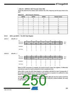
Table 23-3. Voltage Reference Selections for ADC
REFS1
REFS0
Voltage Reference Selection
0
0
1
1
0
1
0
1
AREF, Internal Vref turned off.
AVCC with external capacitor at AREF pin.
Reserved
Internal 2.56V Voltage Reference with external capacitor at AREF pin.
247
8160C–AVR–07/09

 ATMEL [ ATMEL ]