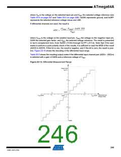
ATmega64A
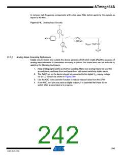
to remove high frequency components with a low-pass filter before applying the signals as
inputs to the ADC.
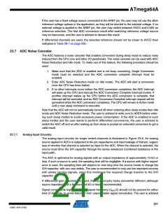
Figure 23-8. Analog Input Circuitry
IIH
ADCn
1..100 kΩ
CS/H= 14 pF
IIL
VCC/2
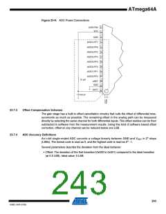
23.7.2
Analog Noise Canceling Techniques
Digital circuitry inside and outside the device generates EMI which might affect the accuracy of
analog measurements. If conversion accuracy is critical, the noise level can be reduced by
applying the following techniques:
1. Keep analog signal paths as short as possible. Make sure analog tracks run over the
ground plane, and keep them well away from high-speed switching digital tracks.
2. The AVCC pin on the device should be connected to the digital VCC supply voltage
via an LC network as shown in Figure 23-9.
3. Use the ADC noise canceler function to reduce induced noise from the CPU.
4. If any ADC port pins are used as digital outputs, it is essential that these do not
switch while a conversion is in progress.
242
8160C–AVR–07/09

 ATMEL [ ATMEL ]