ATmega64A
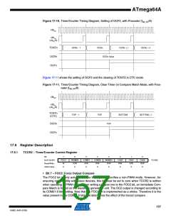
Figure 17-10. Timer/Counter Timing Diagram, Setting of OCF2, with Prescaler (fclk_I/O/8)
clkI/O
clkTn
(clkI/O/8)
TCNTn
OCRn
OCFn
OCRn - 1
OCRn
OCRn + 1
OCRn + 2
OCRn Value
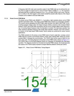
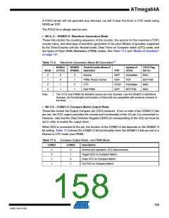
Figure 17-11 shows the setting of OCF2 and the clearing of TCNT2 in CTC mode.
Figure 17-11. Timer/Counter Timing Diagram, Clear Timer on Compare Match Mode, with Pres-
caler (fclk_I/O/8)
clkI/O
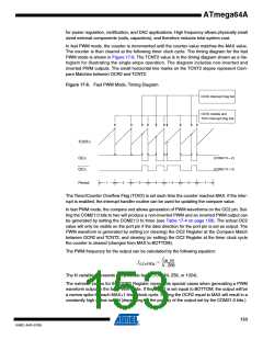
clkTn
(clkI/O/8)
TCNTn
(CTC)
TOP - 1
TOP
BOTTOM
BOTTOM + 1
OCRn
TOP
OCFn
17.9 Register Description
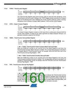
17.9.1
TCCR2 – Timer/Counter Control Register
Bit
7
FOC2
W
6
WGM20
R/W
0
5
COM21
R/W
0
4
3
WGM21
R/W
0
2
CS22
R/W
0
1
CS21
R/W
0
0
0x25 (0x45)
Read/Write
Initial Value
COM20
R/W
0
CS20
R/W
0
TCCR2
0
• Bit 7 – FOC2: Force Output Compare
The FOC2 bit is only active when the WGM20 bit specifies a non-PWM mode. However, for
ensuring compatibility with future devices, this bit must be set to zero when TCCR2 is written
when operating in PWM mode. When writing a logical one to the FOC2 bit, an immediate Com-
pare Match is forced on the waveform generation unit. The OC2 output is changed according to
its COM21:0 bits setting. Note that the FOC2 bit is implemented as a strobe. Therefore it is the
value present in the COM21:0 bits that determines the effect of the forced compare.
157
8160C–AVR–07/09

 ATMEL [ ATMEL ]