ATmega64A
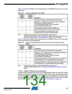
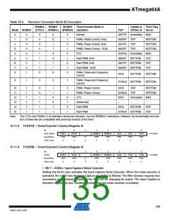
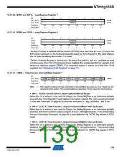
Table 15-5. Waveform Generation Mode Bit Description
WGMn2
(CTCn)
WGMn1
WGMn0
Timer/Counter Mode of
Update of TOVn Flag
OCRnx at Set on
Mode WGMn3
(PWMn1) (PWMn0) Operation
TOP
0
1
2
3
4
5
6
7
8
0
0
0
0
0
0
0
0
1
0
0
0
0
1
1
1
1
0
0
0
1
1
0
0
1
1
0
0
1
0
1
0
1
0
1
0
Normal
0xFFFF Immediate MAX
PWM, Phase Correct, 8-bit
PWM, Phase Correct, 9-bit
PWM, Phase Correct, 10-bit
CTC
0x00FF
0x01FF
0x03FF
OCRnA
0x00FF
0x01FF
0x03FF
TOP
TOP
TOP
BOTTOM
BOTTOM
BOTTOM
Immediate MAX
Fast PWM, 8-bit
BOTTOM
BOTTOM
BOTTOM
TOP
TOP
TOP
Fast PWM, 9-bit
Fast PWM, 10-bit
PWM, Phase and Frequency
Correct
ICRn
BOTTOM
BOTTOM
BOTTOM
BOTTOM
9
1
0
0
1
PWM, Phase and Frequency
Correct
OCRnA
10
11
1
1
1
1
1
1
0
0
1
1
1
1
1
1
0
0
1
1
0
1
0
1
0
1
PWM, Phase Correct
PWM, Phase Correct
CTC
ICRn
OCRnA
ICRn
–
TOP
TOP
BOTTOM
BOTTOM
12
Immediate MAX
13
(Reserved)
–
–
14
Fast PWM
ICRn
OCRnA
BOTTOM
BOTTOM
TOP
TOP
15
Fast PWM
Note:
The CTCn and PWMn1:0 bit definition names are obsolete. Use the WGMn2:0 definitions. However, the functionality and loca-
tion of these bits are compatible with previous versions of the timer.
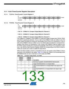
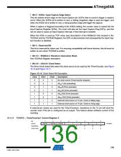
15.11.3 TCCR1B – Timer/Counter1 Control Register B
Bit
7
ICNC1
R/W
0
6
ICES1
R/W
0
5
–
4
WGM13
R/W
0
3
WGM12
R/W
0
2
CS12
R/W
0
1
CS11
R/W
0
0
CS10
R/W
0
0x2E (0x4E)
Read/Write
Initial Value
TCCR1B
R
0
15.11.4 TCCR3B – Timer/Counter3 Control Register B
Bit
7
ICNC3
R/W
0
6
ICES3
R/W
0
5
–
4
WGM33
R/W
0
3
WGM32
R/W
0
2
CS32
R/W
0
1
CS31
R/W
0
0
CS30
R/W
0
(0x8A)
TCCR3B
Read/Write
Initial Value
R
0
• Bit 7 – ICNCn: Input Capture Noise Canceler
Setting this bit (to one) activates the Input Capture Noise Canceler. When the noise canceler is
activated, the input from the Input Capture pin (ICPn) is filtered. The filter function requires four
successive equal valued samples of the ICPn pin for changing its output. The Input Capture is
therefore delayed by four Oscillator cycles when the noise canceler is enabled.
135
8160C–AVR–07/09

 ATMEL [ ATMEL ]