ATmega64A
15.11 16-bit Timer/Counter Register Description
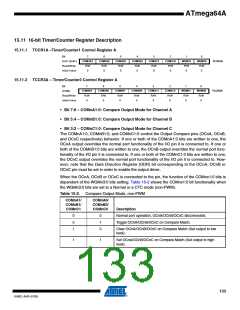
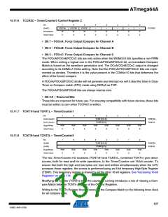
15.11.1 TCCR1A –Timer/Counter1 Control Register A
Bit
7
COM1A1
R/W
6
COM1A0
R/W
5
COM1B1
R/W
4
COM1B0
R/W
3
COM1C1
R/W
2
COM1C0
R/W
1
WGM11
R/W
0
0
WGM10
R/W
0
TCCR1A
0x2F (0x4F)
Read/Write
Initial Value
0
0
0
0
0
0
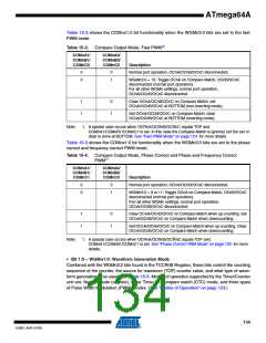
15.11.2 TCCR3A – Timer/Counter3 Control Register A
Bit
7
COM3A1
R/W
6
COM3A0
R/W
5
COM3B1
R/W
4
COM3B0
R/W
3
COM3C1
R/W
2
COM3C0
R/W
1
WGM31
R/W
0
0
WGM30
R/W
0
TCCR3A
(0x8B)
Read/Write
Initial Value
0
0
0
0
0
0
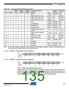
• Bit 7:6 – COMnA1:0: Compare Output Mode for Channel A
• Bit 5:4 – COMnB1:0: Compare Output Mode for Channel B
• Bit 3:2 – COMnC1:0: Compare Output Mode for Channel C
The COMnA1:0, COMnB1:0, and COMnC1:0 control the Output Compare pins (OCnA, OCnB,
and OCnC respectively) behavior. If one or both of the COMnA1:0 bits are written to one, the
OCnA output overrides the normal port functionality of the I/O pin it is connected to. If one or
both of the COMnB1:0 bits are written to one, the OCnB output overrides the normal port func-
tionality of the I/O pin it is connected to. If one or both of the COMnC1:0 bits are written to one,
the OCnC output overrides the normal port functionality of the I/O pin it is connected to. How-
ever, note that the Data Direction Register (DDR) bit corresponding to the OCnA, OCnB or
OCnC pin must be set in order to enable the output driver.
When the OCnA, OCnB or OCnC is connected to the pin, the function of the COMnx1:0 bits is
dependent of the WGMn3:0 bits setting. Table 15-2 shows the COMnx1:0 bit functionality when
the WGMn3:0 bits are set to a Normal or a CTC mode (non-PWM).
Table 15-2. Compare Output Mode, non-PWM
COMnA1/
COMnB1/
COMnC1
COMnA0/
COMnB0/
COMnC0
Description
0
0
1
0
1
0
Normal port operation, OCnA/OCnB/OCnC disconnected.
Toggle OCnA/OCnB/OCnC on Compare Match.
Clear OCnA/OCnB/OCnC on Compare Match (Set output to low
level).
1
1
Set OCnA/OCnB/OCnC on Compare Match (Set output to high
level).
133
8160C–AVR–07/09

 ATMEL [ ATMEL ]