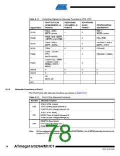
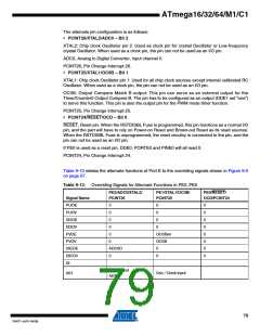
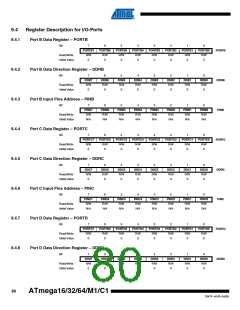
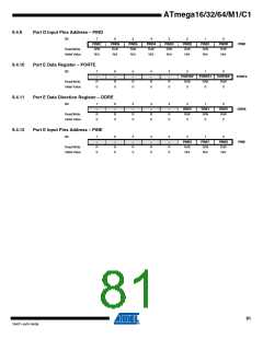
10. External Interrupts
The External Interrupts are triggered by the INT3:0 pins or any of the PCINT23..0 pins. Observe
that, if enabled, the interrupts will trigger even if the INT3:0 or PCINT23..0 pins are configured as
outputs. This feature provides a way of generating a software interrupt. The pin change interrupt
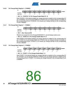
PCI2 will trigger if any enabled PCINT23..16 pin toggles. The pin change interrupt PCI1 will trig-
ger if any enabled PCINT14..8 pin toggles. The pin change interrupt PCI0 will trigger if any
enabled PCINT7..0 pin toggles. The PCMSK3, PCMSK2, PCMSK1 and PCMSK0 Registers
control which pins contribute to the pin change interrupts. Pin change interrupts on PCINT26..0
are detected asynchronously. This implies that these interrupts can be used for waking the part
also from sleep modes other than Idle mode.
The INT3:0 interrupts can be triggered by a falling or rising edge or a low level. This is set up as
indicated in the specification for the External Interrupt Control Register A – EICRA. When the
INT3:0 interrupts are enabled and are configured as level triggered, the interrupts will trigger as
long as the pin is held low. Note that recognition of falling or rising edge interrupts on INT3:0
requires the presence of an I/O clock, described in “Clock Systems and their Distribution” on
page 29. Low level interrupt on INT3:0 is detected asynchronously. This implies that this inter-
rupt can be used for waking the part also from sleep modes other than Idle mode. The I/O clock
is halted in all sleep modes except Idle mode.
Note that if a level triggered interrupt is used for wake-up from Power-down, the required level
must be held long enough for the MCU to complete the wake-up to trigger the level interrupt. If
the level disappears before the end of the Start-up Time, the MCU will still wake up, but no inter-
rupt will be generated. The start-up time is defined by the SUT and CKSEL Fuses as described
in “Clock Systems and their Distribution” on page 29.
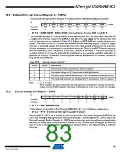
10.1 Pin Change Interrupt Timing
An example of timing of a pin change interrupt is schown in Figure 10-1.
Figure 10-1. Timing of a pin change interrupts
0
pcint_sync
pcint_set/flag
pin_lat
pin_sync
pcint_in[i]
PCINT[i]
pin
PCIFn
(interrupt
flag)
D
Q
D
Q
D
Q
D
Q
D
Q
LE
7
PCINT[i] bit
(of PCMSKn)
clk
clk
clk
PCINT[i] pin
pin_lat
pin_sync
pcint_in[i]
pcint_syn
pcint_set/flag
PCIFn
82
ATmega16/32/64/M1/C1
7647F–AVR–04/09

 ATMEL [ ATMEL ]