ATmega16/32/64/M1/C1
The alternate pin configuration is as follows:
• PCINT26/XTAL2/ADC0 – Bit 2
XTAL2: Chip clock Oscillator pin 2. Used as clock pin for crystal Oscillator or Low-frequency
crystal Oscillator. When used as a clock pin, the pin can not be used as an I/O pin.
ADC0, Analog to Digital Converter, input channel 0.
PCINT26, Pin Change Interrupt 26.
• PCINT25/XTAL1/OC0B – Bit 1
XTAL1: Chip clock Oscillator pin 1. Used for all chip clock sources except internal calibrated RC
Oscillator. When used as a clock pin, the pin can not be used as an I/O pin.
OC0B, Output Compare Match B output: This pin can serve as an external output for the
Timer/Counter0 Output Compare B. The pin has to be configured as an output (DDE1 set “one”)
to serve this function. This pin is also the output pin for the PWM mode timer function.
PCINT25, Pin Change Interrupt 25.
• PCINT24/RESET/OCD – Bit 0
RESET, Reset pin: When the RSTDISBL Fuse is programmed, this pin functions as a normal I/O
pin, and the part will have to rely on Power-on Reset and Brown-out Reset as its reset sources.
When the RSTDISBL Fuse is unprogrammed, the reset circuitry is connected to the pin, and the
pin can not be used as an I/O pin.
If PE0 is used as a reset pin, DDE0, PORTE0 and PINE0 will all read 0.
PCINT24, Pin Change Interrupt 24.
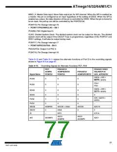
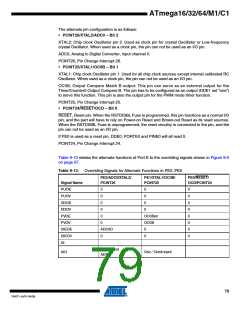
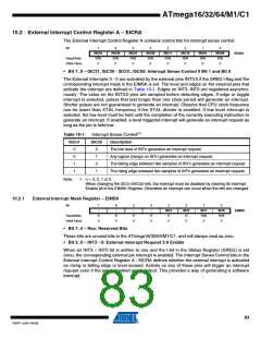
Table 9-13 relates the alternate functions of Port E to the overriding signals shown in Figure 9-5
on page 67.
Table 9-13. Overriding Signals for Alternate Functions in PE2..PE0
PE2/ADC0/XTAL2/
PCINT26
PE1/XTAL1/OC0B/
PCINT25
PE0/RESET/
Signal Name
PUOE
PUOV
DDOE
DDOV
PVOE
PVOV
OCD/PCINT24
0
0
0
0
0
0
0
0
0
0
0
0
0
0
0
0
0
OC0Ben
0
OC0B
DIEOE
DIEOV
DI
ADC0D
0
0
0
Osc Output
ADC0
AIO
Osc / Clock input
79
7647F–AVR–04/09

 ATMEL [ ATMEL ]