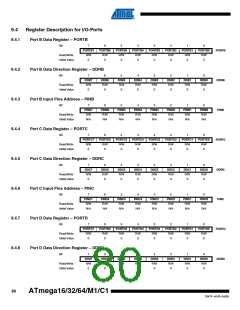
10.2.2
External Interrupt Flag Register – EIFR
Bit
7
–
6
–
5
–
4
–
3
INTF3
R/W
0
2
INTF2
R/W
0
1
INTF1
R/W
0
0
INTF0
R/W
0
EIFR
Read/Write
Initial Value
R
0
R
0
R
0
R
0
• Bit 7..4 – Res: Reserved Bits
These bits are unused bits in the ATmega16/32/64/M1/C1, and will always read as zero.
• Bit 3..0 – INTF3 - INTF0: External Interrupt Flag 3 - 0
When an edge or logic change on the INT3:0 pin triggers an interrupt request, INTF3:0 becomes
set (one). If the I-bit in SREG and the corresponding interrupt enable bit INT3:0 in EIMSK, are
set (one), the MCU will jump to the interrupt vector. The flag is cleared when the interrupt routine
is executed. Alternatively, the flag can be cleared by writing a logical one to it. These flags are
always cleared when INT3:0 are configured as a level interrupt.
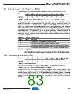
10.2.3
Pin Change Interrupt Control Register - PCICR
Bit
7
6
5
–
4
–
3
PCIE3
R
2
PCIE2
R/W
0
1
PCIE1
R/W
0
0
PCIE0
R/W
0
–
–
PCICR
Read/Write
Initial Value
R
0
R
0
R
0
R
0
0
• Bit 7..4 - Res: Reserved Bits
These bits are unused bits in the ATmega16/32/64/M1/C1, and will always read as zero.
• Bit 3 - PCIE3: Pin Change Interrupt Enable 3
When the PCIE3 bit is set (one) and the I-bit in the Status Register (SREG) is set (one), pin
change interrupt 3 is enabled. Any change on any enabled PCINT26..24 pin will cause an inter-
rupt. The corresponding interrupt of Pin Change Interrupt Request is executed from the PCI3
Interrupt Vector. PCINT26..24 pins are enabled individually by the PCMSK3 Register.
• Bit 2 - PCIE2: Pin Change Interrupt Enable 2
When the PCIE2 bit is set (one) and the I-bit in the Status Register (SREG) is set (one), pin
change interrupt 2 is enabled. Any change on any enabled PCINT23..16 pin will cause an inter-
rupt. The corresponding interrupt of Pin Change Interrupt Request is executed from the PCI2
Interrupt Vector. PCINT23..16 pins are enabled individually by the PCMSK2 Register.
• Bit 1 - PCIE1: Pin Change Interrupt Enable 1
When the PCIE1 bit is set (one) and the I-bit in the Status Register (SREG) is set (one), pin
change interrupt 1 is enabled. Any change on any enabled PCINT15..8 pin will cause an inter-
rupt. The corresponding interrupt of Pin Change Interrupt Request is executed from the PCI1
Interrupt Vector. PCINT15..8 pins are enabled individually by the PCMSK1 Register.
• Bit 0 - PCIE0: Pin Change Interrupt Enable 0
When the PCIE0 bit is set (one) and the I-bit in the Status Register (SREG) is set (one), pin
change interrupt 0 is enabled. Any change on any enabled PCINT7..0 pin will cause an interrupt.
The corresponding interrupt of Pin Change Interrupt Request is executed from the PCI0 Inter-
rupt Vector. PCINT7..0 pins are enabled individually by the PCMSK0 Register.
84
ATmega16/32/64/M1/C1
7647F–AVR–04/09

 ATMEL [ ATMEL ]