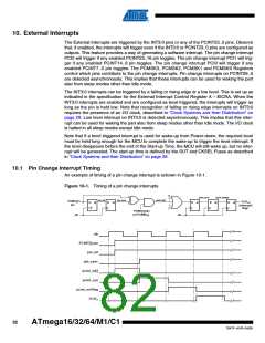
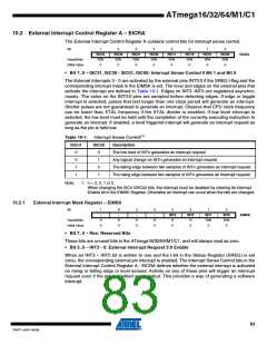
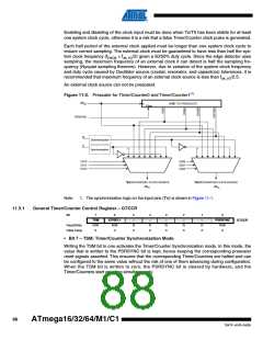
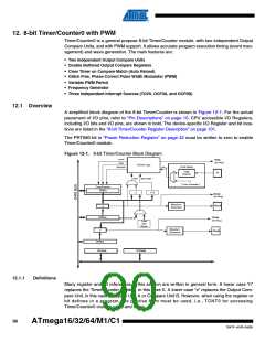
10.2.6
Pin Change Mask Register 2 – PCMSK2
Bit
7
PCINT23
R/W
0
6
PCINT22
R/W
0
5
PCINT21
R/W
0
4
PCINT20
R/W
0
3
PCINT19
R/W
0
2
PCINT18
R/W
0
1
PCINT17
R/W
0
0
PCINT16
R/W
0
PCMSK2
Read/Write
Initial Value
• Bit 7..0 – PCINT23..16: Pin Change Enable Mask 23..16
Each PCINT23..16-bit selects whether pin change interrupt is enabled on the corresponding I/O
pin. If PCINT23..16 is set and the PCIE2 bit in PCICR is set, pin change interrupt is enabled on
the corresponding I/O pin. If PCINT23..16 is cleared, pin change interrupt on the corresponding
I/O pin is disabled.
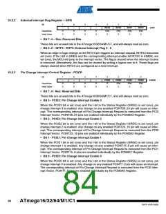
10.2.7
Pin Change Mask Register 1 – PCMSK1
Bit
7
6
PCINT14
R/W
0
5
PCINT13
R/W
0
4
PCINT12
R/W
0
3
PCINT11
R/W
0
2
PCINT10
R/W
0
1
PCINT9
R/W
0
0
PCINT8
R/W
0
PCINT15
PCMSK1
Read/Write
Initial Value
R
0
• Bit 7 – Res: Reserved Bit
This bit is an unused bit in the ATmega16/32/64/M1/C1, and will always read as zero.
• Bit 7..0 – PCINT15..8: Pin Change Enable Mask 15..8
Each PCINT15..8-bit selects whether pin change interrupt is enabled on the corresponding I/O
pin. If PCINT15..8 is set and the PCIE1 bit in PCICR is set, pin change interrupt is enabled on
the corresponding I/O pin. If PCINT15..8 is cleared, pin change interrupt on the corresponding
I/O pin is disabled.
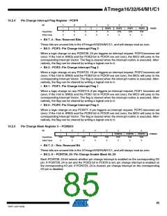
10.2.8
Pin Change Mask Register 0 – PCMSK0
Bit
7
6
5
4
3
2
1
0
PCINT7
R/W
0
PCINT6
R/W
0
PCINT5
R/W
0
PCINT4
R/W
0
PCINT3
R/W
0
PCINT2
R/W
0
PCINT1
R/W
0
PCINT0
R/W
0
PCMSK0
Read/Write
Initial Value
• Bit 7..0 – PCINT7..0: Pin Change Enable Mask 7..0
Each PCINT7..0 bit selects whether pin change interrupt is enabled on the corresponding I/O
pin. If PCINT7..0 is set and the PCIE0 bit in PCICR is set, pin change interrupt is enabled on the
corresponding I/O pin. If PCINT7..0 is cleared, pin change interrupt on the corresponding I/O pin
is disabled.
86
ATmega16/32/64/M1/C1
7647F–AVR–04/09

 ATMEL [ ATMEL ]