ATmega16/32/64/M1/C1
MISO_A: Master Data input, Slave Data output pin for SPI channel. When the SPI is enabled as
a master, this pin is configured as an input regardless of the setting of DDD2. When the SPI is
enabled as a slave, the data direction of this pin is controlled by DDD2. When the pin is forced to
be an input, the pull-up can still be controlled by the PORTD2 bit.
PCINT18, Pin Change Interrupt 18.
• PCINT17/PSCIN0/CLKO – Bit 1
PCSIN0, PSC Digital Input 0.
CLKO, Divided System Clock: The divided system clock can be output on this pin. The divided
system clock will be output if the CKOUT Fuse is programmed, regardless of the PORTD1 and
DDD1 settings. It will also be output during reset.
PCINT17, Pin Change Interrupt 17.
• PCINT16/PSCOUT0A – Bit 0
PSCOUT0A: Output 0 of PSC 0.
PCINT16, Pin Change Interrupt 16.
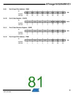
Table 9-10 and Table 9-11 relates the alternate functions of Port D to the overriding signals
shown in Figure 9-5 on page 67.
Table 9-10. Overriding Signals for Alternate Functions PD7..PD4
PD7/
PD6/ADC3/
ACMPN2/INT0/
PCINT22
PD4/ADC1/RXD/
RXLIN/ICP1A/
ACMP0/
PCINT23
PD5/ADC2/
Signal Name
ACMP2/PCINT21
SCK_A/PCINT20
RXEN + SPE •
MSTR • SPIPS
PUOE
0
0
0
0
0
0
PD4 •
PUD
PUOV
RXEN + SPE •
MSTR • SPIPS
DDOE
DDOV
PVOE
0
0
0
0
0
0
0
0
0
0
SPE • MSTR •
SPIPS
PVOV
DIEOE
DIEOV
DI
0
0
0
–
ACMP0D
ADC3D + In0en
In0en
ADC2D
0
ADC1D
0
0
–
INT0
ICP1A
ADC3
ADC2
AIO
ACOMP0
ADC1
ACMPM
ACOMP2
77
7647F–AVR–04/09

 ATMEL [ ATMEL ]