ATmega16/32/64/M1/C1
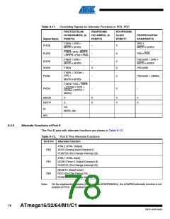
9.3.4
Alternate Functions of Port D
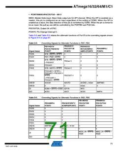
The Port D pins with alternate functions are shown in Table 9-9.
Table 9-9.
Port Pin
Port D Pins Alternate Functions
Alternate Function
ACMP0 (Analog Comparator 0 Positive Input )
PCINT23 (Pin Change Interrupt 23)
PD7
ADC3 (Analog Input Channel 3 )
ACMPN2 (Analog Comparator 2 Negative Input)
INT0 (External Interrupt 0)
PD6
PCINT22 (Pin Change Interrupt 22)
ADC2 (Analog Input Channel 2)
PD5
PD4
ACMP2 (Analog Comparator 2 Positive Input )
PCINT21 (Pin Change Interrupt 21)
ADC1 (Analog Input Channel 1)
RXD/RXLIN (LIN/UART Rx data)
ICP1A (Timer 1 input capture)
SCK_A (Programming & alternate SPI Clock)
PCINT20 (Pin Change Interrupt 20)
TXD/TXLIN (LIN/UART Tx data)
OC0A (Timer 0 Output Compare A)
SS (SPI Slave Select)
PD3
PD2
MOSI_A (Programming & alternate SPI Master Out Slave In)
PCINT19 (Pin Change Interrupt 19)
PSCIN2 (PSC Digital Input 2)
OC1A (Timer 1 Output Compare A)
MISO_A (Programming & alternate Master In SPI Slave Out)
PCINT18 (Pin Change Interrupt 18)
PSCIN0 (PSC Digital Input 0)
CLKO (System Clock Output)
PCINT17 (Pin Change Interrupt 17)
PD1
PD0
PSCOUT0A (PSC output 0A)
PCINT16 (Pin Change Interrupt 16)
The alternate pin configuration is as follows:
• ACMP0/PCINT23 – Bit 7
ACMP0, Analog Comparator 0 Positive Input. Configure the port pin as input with the internal
pull-up switched off to avoid the digital port function from interfering with the function of the Ana-
log Comparator.
PCINT23, Pin Change Interrupt 23.
• ADC3/ACMPN2/INT0/PCINT22 – Bit 6
ADC3, Analog to Digital Converter, input channel 3.
75
7647F–AVR–04/09

 ATMEL [ ATMEL ]