ATmega16/32/64/M1/C1
• Bit 6:1 – BRP5:0: Baud Rate Prescaler
The period of the CAN controller system clock Tscl is programmable and determines the individ-
ual bit timing.
BRP[5:0] + 1
Tscl = --------------------------------------
clkIOfrequency
If ‘BRP[5..0]=0’, see Section 16.4.3 “Baud Rate” on page 177 and Section • “Bit 0 – SMP: Sam-
ple Point(s)” on page 194.
• Bit 0 – Reserved Bit
This bit is reserved for future use. For compatibility with future devices, it must be written to zero
when CANBT1 is written.
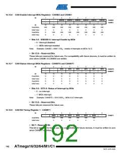
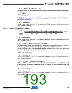
16.10.9 CAN Bit Timing Register 2 - CANBT2
Bit
7
6
SJW1
R/W
0
5
SJW0
R/W
0
4
-
3
PRS2
R/W
0
2
PRS1
R/W
0
1
PRS0
R/W
0
0
-
-
-
-
CANBT2
Read/Write
Initial Value
-
-
-
-
• Bit 7– Reserved Bit
This bit is reserved for future use. For compatibility with future devices, it must be written to zero
when CANBT2 is written.
• Bit 6:5 – SJW1:0: Re-Synchronization Jump Width
To compensate for phase shifts between clock oscillators of different bus controllers, the control-
ler must re-synchronize on any relevant signal edge of the current transmission.
The synchronization jump width defines the maximum number of clock cycles. A bit period may
be shortened or lengthened by a re-synchronization.
Tsjw = Tscl × (SJW[1:0] + 1)
• Bit 4 – Reserved Bit
This bit is reserved for future use. For compatibility with future devices, it must be written to zero
when CANBT2 is written.
• Bit 3:1 – PRS2:0: Propagation Time Segment
This part of the bit time is used to compensate for the physical delay times within the network. It
is twice the sum of the signal propagation time on the bus line, the input comparator delay and
the output driver delay.
Tprs = Tscl × (PRS[2:0] + 1)
• Bit 0 – Reserved Bit
This bit is reserved for future use. For compatibility with future devices, it must be written to zero
when CANBT2 is written.
193
7647F–AVR–04/09

 ATMEL [ ATMEL ]