ATmega8(L)
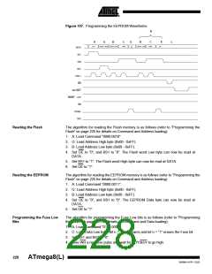
Chip Erase
The Chip Erase will erase the Flash and EEPROM(1) memories plus Lock Bits. The Lock
Bits are not reset until the Program memory has been completely erased. The Fuse Bits
are not changed. A Chip Erase must be performed before the Flash and/or the
EEPROM are reprogrammed.
Note:
1. The EEPRPOM memory is preserved during chip erase if the EESAVE Fuse is
programmed.
Load Command “Chip Erase”
1. Set XA1, XA0 to “10”. This enables command loading.
2. Set BS1 to “0”.
3. Set DATA to “1000 0000”. This is the command for Chip Erase.
4. Give XTAL1 a positive pulse. This loads the command.
5. Give WR a negative pulse. This starts the Chip Erase. RDY/BSY goes low.
6. Wait until RDY/BSY goes high before loading a new command.
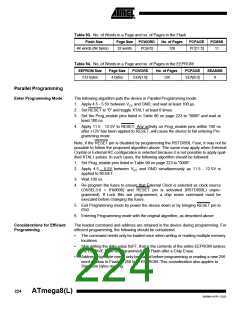
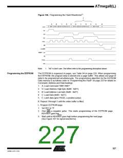
Programming the Flash
The Flash is organized in pages, see Table 93 on page 224. When programming the
Flash, the program data is latched into a page buffer. This allows one page of program
data to be programmed simultaneously. The following procedure describes how to pro-
gram the entire Flash memory:
A. Load Command “Write Flash”
1. Set XA1, XA0 to “10”. This enables command loading.
2. Set BS1 to ”0”.
3. Set DATA to “0001 0000”. This is the command for Write Flash.
4. Give XTAL1 a positive pulse. This loads the command.
B. Load Address Low byte
1. Set XA1, XA0 to “00”. This enables address loading.
2. Set BS1 to “0”. This selects low address.
3. Set DATA = Address Low byte (0x00 - 0xFF).
4. Give XTAL1 a positive pulse. This loads the address Low byte.
C. Load Data Low byte
1. Set XA1, XA0 to “01”. This enables data loading.
2. Set DATA = Data Low byte (0x00 - 0xFF).
3. Give XTAL1 a positive pulse. This loads the data byte.
D. Load Data High byte
1. Set BS1 to “1”. This selects high data byte.
2. Set XA1, XA0 to “01”. This enables data loading.
3. Set DATA = Data High byte (0x00 - 0xFF).
4. Give XTAL1 a positive pulse. This loads the data byte.
E. Latch Data
1. Set BS1 to “1”. This selects high data byte.
2. Give PAGEL a positive pulse. This latches the data bytes. (See Figure 106 for
signal waveforms)
F. Repeat B through E until the entire buffer is filled or until all data within the page is
loaded.
225
2486M–AVR–12/03

 ATMEL [ ATMEL ]