Parallel Programming
Parameters, Pin
Mapping, and
This section describes how to parallel program and verify Flash Program memory,
EEPROM Data memory, Memory Lock Bits, and Fuse Bits in the ATmega8. Pulses are
assumed to be at least 250 ns unless otherwise noted.
Commands
Signal Names
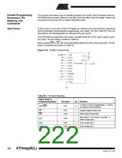
In this section, some pins of the ATmega8 are referenced by signal names describing
their functionality during parallel programming, see Figure 104 and Table 89. Pins not
described in the following table are referenced by pin names.
The XA1/XA0 pins determine the action executed when the XTAL1 pin is given a posi-
tive pulse. The bit coding is shown in Table 91.
When pulsing WR or OE, the command loaded determines the action executed. The dif-
ferent Commands are shown in Table 92.
Figure 104. Parallel Programming
+5V
RDY/BSY
OE
PD1
PD2
PD3
PD4
PD5
PD6
PD7
VCC
+5V
AVCC
WR
BS1
PC[1:0]:PB[5:0]
DATA
XA0
XA1
PAGEL
+12 V
BS2
RESET
PC2
XTAL1
GND
Table 89. Pin Name Mapping
Signal Name in
Programming Mode
Pin Name
I/O Function
0: Device is busy programming, 1: Device
is ready for new command
RDY/BSY
PD1
O
OE
PD2
PD3
I
I
Output Enable (Active low)
Write Pulse (Active low)
WR
Byte Select 1 (“0” selects Low byte, “1”
selects High byte)
BS1
PD4
I
XA0
XA1
PD5
PD6
I
I
XTAL Action Bit 0
XTAL Action Bit 1
222
ATmega8(L)
2486M–AVR–12/03

 ATMEL [ ATMEL ]