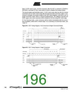
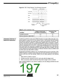
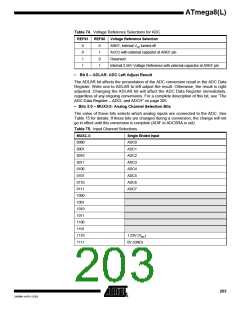
ATmega8(L)
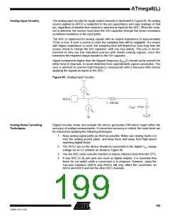
Analog Input Circuitry
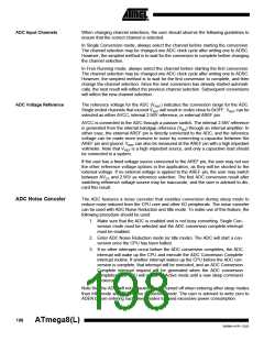
The analog input circuitry for single ended channels is illustrated in Figure 95. An analog
source applied to ADCn is subjected to the pin capacitance and input leakage of that
pin, regardless of whether that channel is selected as input for the ADC. When the chan-
nel is selected, the source must drive the S/H capacitor through the series resistance
(combined resistance in the input path).
The ADC is optimized for analog signals with an output impedance of approximately
10 kΩ or less. If such a source is used, the sampling time will be negligible. If a source
with higher impedance is used, the sampling time will depend on how long time the
source needs to charge the S/H capacitor, with can vary widely. The user is recom-
mended to only use low impedant sources with slowly varying signals, since this
minimizes the required charge transfer to the S/H capacitor.
Signal components higher than the Nyquist frequency (fADC/2) should not be present for
either kind of channels, to avoid distortion from unpredictable signal convolution. The
user is advised to remove high frequency components with a low-pass filter before
applying the signals as inputs to the ADC.
Figure 95. Analog Input Circuitry
IIH
ADCn
1..100 kΩ
CS/H= 14 pF
IIL
VCC/2
Analog Noise Canceling
Techniques
Digital circuitry inside and outside the device generates EMI which might affect the
accuracy of analog measurements. If conversion accuracy is critical, the noise level can
be reduced by applying the following techniques:
1. Keep analog signal paths as short as possible. Make sure analog tracks run
over the analog ground plane, and keep them well away from high-speed
switching digital tracks.
2. The AVCC pin on the device should be connected to the digital VCC supply
voltage via an LC network as shown in Figure 96.
3. Use the ADC noise canceler function to reduce induced noise from the CPU.
4. If any ADC [3..0] port pins are used as digital outputs, it is essential that
these do not switch while a conversion is in progress. However, using the
Two-wire Interface (ADC4 and ADC5) will only affect the conversion on
ADC4 and ADC5 and not the other ADC channels.
199
2486M–AVR–12/03

 ATMEL [ ATMEL ]