ATmega8(L)
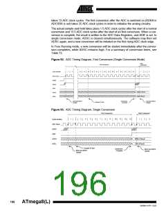
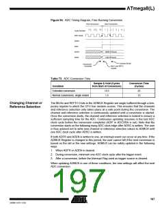
Figure 94. ADC Timing Diagram, Free Running Conversion
One Conversion
Next Conversion
11
12
13
1
2
3
4
Cycle Number
ADC Clock
ADSC
ADIF
ADCH
ADCL
MSB of Result
LSB of Result
Sample &Hold
MUX and REFS
Update
Conversion
Complete
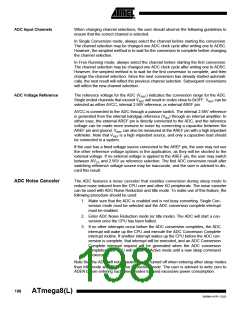
Table 73. ADC Conversion Time
Sample & Hold (Cycles
from Start of Conversion)
Conversion Time
(Cycles)
Condition
Extended conversion
Normal conversions, single ended
13.5
1.5
25
13
Changing Channel or
Reference Selection
The MUXn and REFS1:0 bits in the ADMUX Register are single buffered through a tem-
porary register to which the CPU has random access. This ensures that the channels
and reference selection only takes place at a safe point during the conversion. The
channel and reference selection is continuously updated until a conversion is started.
Once the conversion starts, the channel and reference selection is locked to ensure a
sufficient sampling time for the ADC. Continuous updating resumes in the last ADC
clock cycle before the conversion completes (ADIF in ADCSRA is set). Note that the
conversion starts on the following rising ADC clock edge after ADSC is written. The user
is thus advised not to write new channel or reference selection values to ADMUX until
one ADC clock cycle after ADSC is written.
If both ADFR and ADEN is written to one, an interrupt event can occur at any time. If the
ADMUX Register is changed in this period, the user cannot tell if the next conversion is
based on the old or the new settings. ADMUX can be safely updated in the following
ways:
1. When ADFR or ADEN is cleared.
2. During conversion, minimum one ADC clock cycle after the trigger event.
3. After a conversion, before the Interrupt Flag used as trigger source is cleared.
When updating ADMUX in one of these conditions, the new settings will affect the next
ADC conversion.
197
2486M–AVR–12/03

 ATMEL [ ATMEL ]