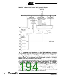
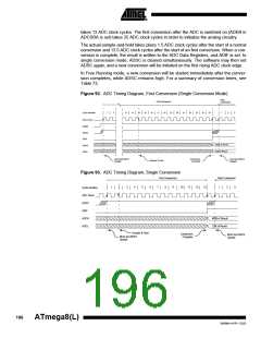
takes 13 ADC clock cycles. The first conversion after the ADC is switched on (ADEN in
ADCSRA is set) takes 25 ADC clock cycles in order to initialize the analog circuitry.
The actual sample-and-hold takes place 1.5 ADC clock cycles after the start of a normal
conversion and 13.5 ADC clock cycles after the start of an first conversion. When a con-
version is complete, the result is written to the ADC Data Registers, and ADIF is set. In
single conversion mode, ADSC is cleared simultaneously. The software may then set
ADSC again, and a new conversion will be initiated on the first rising ADC clock edge.
In Free Running mode, a new conversion will be started immediately after the conver-
sion completes, while ADSC remains high. For a summary of conversion times, see
Table 73.
Figure 92. ADC Timing Diagram, First Conversion (Single Conversion Mode)
Next
First Conversion
Conversion
Cycle Number
1
2
12
13
14
15
16
17
18
19
20
21
22
23
24
25
1
2
3
ADC Clock
ADEN
ADSC
ADIF
MSB of Result
LSB of Result
ADCH
ADCL
MUX and REFS
Update
Conversion
Complete
MUX and REFS
Update
Sample & Hold
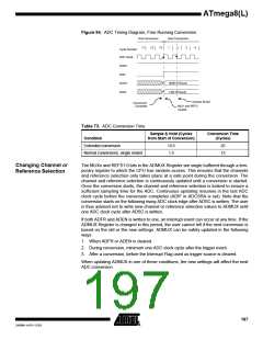
Figure 93. ADC Timing Diagram, Single Conversion
One Conversion
Next Conversion
1
2
3
4
5
6
7
8
9
10
11
12
13
1
2
3
Cycle Number
ADC Clock
ADSC
ADIF
ADCH
MSB of Result
LSB of Result
ADCL
Sample & Hold
Conversion
Complete
MUX and REFS
Update
MUX and REFS
Update
196
ATmega8(L)
2486M–AVR–12/03

 ATMEL [ ATMEL ]