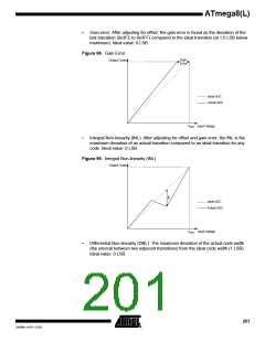
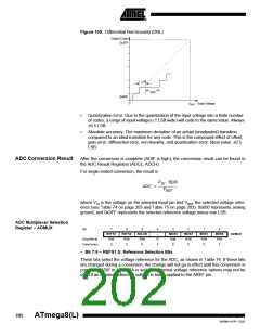
Figure 100. Differential Non-linearity (DNL)
Output Code
0x3FF
1 LSB
DNL
0x000
0
VREF Input Voltage
•
•
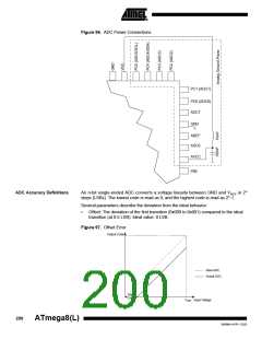
Quantization Error: Due to the quantization of the input voltage into a finite number
of codes, a range of input voltages (1 LSB wide) will code to the same value. Always
±0.5 LSB.
Absolute accuracy: The maximum deviation of an actual (unadjusted) transition
compared to an ideal transition for any code. This is the compound effect of offset,
gain error, differential error, non-linearity, and quantization error. Ideal value: ±0.5
LSB.
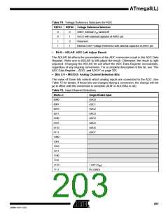
ADC Conversion Result
After the conversion is complete (ADIF is high), the conversion result can be found in
the ADC Result Registers (ADCL, ADCH).
For single ended conversion, the result is
V
1024
IN
ADC = --------------------------
V
REF
where VIN is the voltage on the selected input pin and VREF the selected voltage refer-
ence (see Table 74 on page 203 and Table 75 on page 203). 0x000 represents analog
ground, and 0x3FF represents the selected reference voltage minus one LSB.
ADC Multiplexer Selection
Register – ADMUX
Bit
7
REFS1
R/W
0
6
REFS0
R/W
0
5
ADLAR
R/W
0
4
–
3
MUX3
R/W
0
2
MUX2
R/W
0
1
MUX1
R/W
0
0
MUX0
R/W
0
ADMUX
Read/Write
Initial Value
R
0
• Bit 7:6 – REFS1:0: Reference Selection Bits
These bits select the voltage reference for the ADC, as shown in Table 74. If these bits
are changed during a conversion, the change will not go in effect until this conversion is
complete (ADIF in ADCSRA is set). The internal voltage reference options may not be
used if an external reference voltage is being applied to the AREF pin.
202
ATmega8(L)
2486M–AVR–12/03

 ATMEL [ ATMEL ]