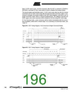
ATmega8(L)
If the result is left adjusted and no more than 8-bit precision is required, it is sufficient to
read ADCH. Otherwise, ADCL must be read first, then ADCH, to ensure that the content
of the Data Registers belongs to the same conversion. Once ADCL is read, ADC access
to Data Registers is blocked. This means that if ADCL has been read, and a conversion
completes before ADCH is read, neither register is updated and the result from the con-
version is lost. When ADCH is read, ADC access to the ADCH and ADCL Registers is
re-enabled.
The ADC has its own interrupt which can be triggered when a conversion completes.
When ADC access to the Data Registers is prohibited between reading of ADCH and
ADCL, the interrupt will trigger even if the result is lost.
Starting a Conversion
A single conversion is started by writing a logical one to the ADC Start Conversion bit,
ADSC. This bit stays high as long as the conversion is in progress and will be cleared by
hardware when the conversion is completed. If a different data channel is selected while
a conversion is in progress, the ADC will finish the current conversion before performing
the channel change.
In Free Running mode, the ADC is constantly sampling and updating the ADC Data
Register. Free Running mode is selected by writing the ADFR bit in ADCSRA to one.
The first conversion must be started by writing a logical one to the ADSC bit in ADC-
SRA. In this mode the ADC will perform successive conversions independently of
whether the ADC Interrupt Flag, ADIF is cleared or not.
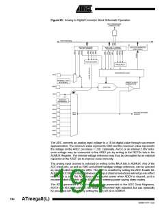
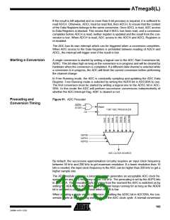
Prescaling and
Figure 91. ADC Prescaler
Conversion Timing
ADEN
START
Reset
7-BIT ADC PRESCALER
CK
ADPS0
ADPS1
ADPS2
ADC CLOCK SOURCE
By default, the successive approximation circuitry requires an input clock frequency
between 50 kHz and 200 kHz to get maximum resolution. If a lower resolution than 10
bits is needed, the input clock frequency to the ADC can be higher than 200 kHz to get a
higher sample rate.
The ADC module contains a prescaler, which generates an acceptable ADC clock fre-
quency from any CPU frequency above 100 kHz. The prescaling is set by the ADPS bits
in ADCSRA. The prescaler starts counting from the moment the ADC is switched on by
setting the ADEN bit in ADCSRA. The prescaler keeps running for as long as the ADEN
bit is set, and is continuously reset when ADEN is low.
When initiating a single ended conversion by setting the ADSC bit in ADCSRA, the con-
version starts at the following rising edge of the ADC clock cycle. A normal conversion
195
2486M–AVR–12/03

 ATMEL [ ATMEL ]