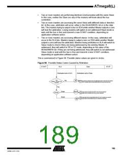
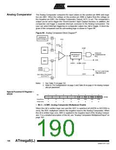
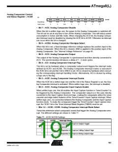
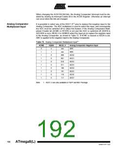
ATmega8(L)
Analog-to-Digital
Converter
Features
• 10-bit Resolution (8-bit Accuracy on ADC4 and ADC5)
• 0.5 LSB Integral Non-linearity
• ± 2 LSB Absolute Accuracy
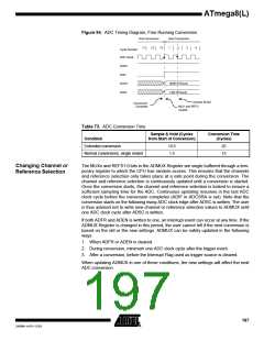
• 65 - 260 µs Conversion Time
• Up to 15 kSPS at Maximum Resolution
• 6 Multiplexed Single Ended Input Channels
• 2 Additional Multiplexed Single Ended Input Channels (TQFP and MLF Package only)
• Optional Left Adjustment for ADC Result Readout
• 0 - VCC ADC Input Voltage Range
• Selectable 2.56V ADC Reference Voltage
• Free Running or Single Conversion Mode
• Interrupt on ADC Conversion Complete
• Sleep Mode Noise Canceler
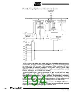
The ATmega8 features a 10-bit successive approximation ADC. The ADC is connected
to an 8-channel Analog Multiplexer which allows eight single-ended voltage inputs con-
structed from the pins of Port C. The single-ended voltage inputs refer to 0V (GND).
Note that ADC channels ADC4 and ADC5 are limited to 8-bit accuracy. Channels
ADC[3:0] and ADC[7:6] offer full 10-bit accuracy.
The ADC contains a Sample and Hold circuit which ensures that the input voltage to the
ADC is held at a constant level during conversion. A block diagram of the ADC is shown
in Figure 90.
The ADC has a separate analog supply voltage pin, AVCC. AVCC must not differ more
than ± 0.3V from VCC. See the paragraph “ADC Noise Canceler” on page 198 on how to
connect this pin.
Internal reference voltages of nominally 2.56V or AVCC are provided On-chip. The volt-
age reference may be externally decoupled at the AREF pin by a capacitor for better
noise performance.
193
2486M–AVR–12/03

 ATMEL [ ATMEL ]