ATmega48/88/168
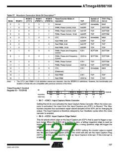
Table 57. Waveform Generation Mode Bit Description(1)
WGM12
(CTC1)
WGM11
WGM10
Timer/Counter Mode of
Update of
OCR1x at
TOV1 Flag
Set on
Mode
WGM13
(PWM11) (PWM10) Operation
TOP
0
1
2
3
4
5
6
7
8
0
0
0
0
0
0
0
0
1
0
0
0
0
1
1
1
1
0
0
0
1
1
0
0
1
1
0
0
1
0
1
0
1
0
1
0
Normal
0xFFFF
0x00FF
0x01FF
0x03FF
OCR1A
0x00FF
0x01FF
0x03FF
ICR1
Immediate
TOP
MAX
PWM, Phase Correct, 8-bit
PWM, Phase Correct, 9-bit
PWM, Phase Correct, 10-bit
CTC
BOTTOM
BOTTOM
BOTTOM
MAX
TOP
TOP
Immediate
TOP
Fast PWM, 8-bit
TOP
Fast PWM, 9-bit
TOP
TOP
Fast PWM, 10-bit
TOP
TOP
PWM, Phase and Frequency
Correct
BOTTOM
BOTTOM
9
1
0
0
1
PWM, Phase and Frequency
Correct
OCR1A
BOTTOM
BOTTOM
10
11
12
13
14
15
1
1
1
1
1
1
0
0
1
1
1
1
1
1
0
0
1
1
0
1
0
1
0
1
PWM, Phase Correct
PWM, Phase Correct
CTC
ICR1
OCR1A
ICR1
–
TOP
TOP
Immediate
–
BOTTOM
BOTTOM
MAX
(Reserved)
–
Fast PWM
ICR1
OCR1A
TOP
TOP
TOP
Fast PWM
TOP
Note:
1. The CTC1 and PWM11:0 bit definition names are obsolete. Use the WGM12:0 definitions. However, the functionality and
location of these bits are compatible with previous versions of the timer.
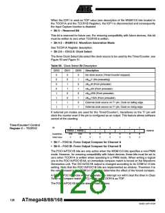
Timer/Counter1 Control
Register B – TCCR1B
Bit
7
ICNC1
R/W
0
6
ICES1
R/W
0
5
–
4
WGM13
R/W
0
3
WGM12
R/W
0
2
CS12
R/W
0
1
CS11
R/W
0
0
CS10
R/W
0
TCCR1B
Read/Write
Initial Value
R
0
• Bit 7 – ICNC1: Input Capture Noise Canceler
Setting this bit (to one) activates the Input Capture Noise Canceler. When the noise can-
celer is activated, the input from the Input Capture pin (ICP1) is filtered. The filter
function requires four successive equal valued samples of the ICP1 pin for changing its
output. The Input Capture is therefore delayed by four Oscillator cycles when the noise
canceler is enabled.
• Bit 6 – ICES1: Input Capture Edge Select
This bit selects which edge on the Input Capture pin (ICP1) that is used to trigger a cap-
ture event. When the ICES1 bit is written to zero, a falling (negative) edge is used as
trigger, and when the ICES1 bit is written to one, a rising (positive) edge will trigger the
capture.
When a capture is triggered according to the ICES1 setting, the counter value is copied
into the Input Capture Register (ICR1). The event will also set the Input Capture Flag
(ICF1), and this can be used to cause an Input Capture Interrupt, if this interrupt is
enabled.
127
2545D–AVR–07/04

 ATMEL [ ATMEL ]