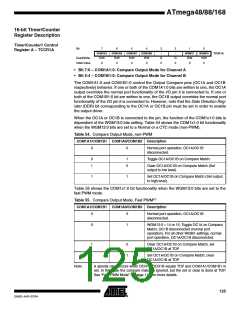
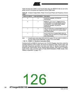
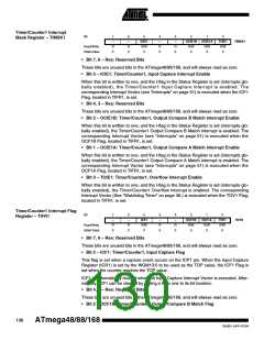
Table 56 shows the COM1x1:0 bit functionality when the WGM13:0 bits are set to the
phase correct or the phase and frequency correct, PWM mode.
Table 56. Compare Output Mode, Phase Correct and Phase and Frequency Correct
PWM(1)
COM1A1/COM1B1 COM1A0/COM1B0 Description
0
0
Normal port operation, OC1A/OC1B
disconnected.
0
1
WGM13:0 = 8, 9, 10 or 11: Toggle OC1A on
Compare Match, OC1B disconnected (normal
port operation). For all other WGM1 settings,
normal port operation, OC1A/OC1B
disconnected.
1
1
0
1
Clear OC1A/OC1B on Compare Match when up-
counting. Set OC1A/OC1B on Compare Match
when downcounting.
Set OC1A/OC1B on Compare Match when up-
counting. Clear OC1A/OC1B on Compare Match
when downcounting.
Note:
1. A special case occurs when OCR1A/OCR1B equals TOP and COM1A1/COM1B1 is
set. See “Phase Correct PWM Mode” on page 119. for more details.
• Bit 1:0 – WGM11:0: Waveform Generation Mode
Combined with the WGM13:2 bits found in the TCCR1B Register, these bits control the
counting sequence of the counter, the source for maximum (TOP) counter value, and
what type of waveform generation to be used, see Table 57. Modes of operation sup-
ported by the Timer/Counter unit are: Normal mode (counter), Clear Timer on Compare
match (CTC) mode, and three types of Pulse Width Modulation (PWM) modes. (See
“Modes of Operation” on page 115.).
126
ATmega48/88/168
2545D–AVR–07/04

 ATMEL [ ATMEL ]