ATmega48/88/168
16-bit Timer/Counter
Register Description
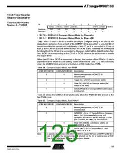
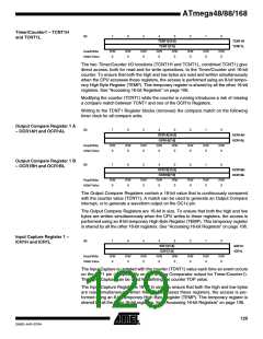
Timer/Counter1 Control
Register A – TCCR1A
Bit
7
COM1A1
R/W
6
COM1A0
R/W
5
COM1B1
R/W
4
COM1B0
R/W
3
–
2
–
1
WGM11
R/W
0
0
WGM10
R/W
0
TCCR1A
Read/Write
Initial Value
R
0
R
0
0
0
0
0
• Bit 7:6 – COM1A1:0: Compare Output Mode for Channel A
• Bit 5:4 – COM1B1:0: Compare Output Mode for Channel B
The COM1A1:0 and COM1B1:0 control the Output Compare pins (OC1A and OC1B
respectively) behavior. If one or both of the COM1A1:0 bits are written to one, the OC1A
output overrides the normal port functionality of the I/O pin it is connected to. If one or
both of the COM1B1:0 bit are written to one, the OC1B output overrides the normal port
functionality of the I/O pin it is connected to. However, note that the Data Direction Reg-
ister (DDR) bit corresponding to the OC1A or OC1B pin must be set in order to enable
the output driver.
When the OC1A or OC1B is connected to the pin, the function of the COM1x1:0 bits is
dependent of the WGM13:0 bits setting. Table 54 shows the COM1x1:0 bit functionality
when the WGM13:0 bits are set to a Normal or a CTC mode (non-PWM).
Table 54. Compare Output Mode, non-PWM
COM1A1/COM1B1 COM1A0/COM1B0 Description
0
0
Normal port operation, OC1A/OC1B
disconnected.
0
1
1
0
Toggle OC1A/OC1B on Compare Match.
Clear OC1A/OC1B on Compare Match (Set
output to low level).
1
1
Set OC1A/OC1B on Compare Match (Set output
to high level).
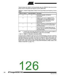
Table 55 shows the COM1x1:0 bit functionality when the WGM13:0 bits are set to the
fast PWM mode.
Table 55. Compare Output Mode, Fast PWM(1)
COM1A1/COM1B1 COM1A0/COM1B0 Description
0
0
Normal port operation, OC1A/OC1B
disconnected.
0
1
WGM13:0 = 14 or 15: Toggle OC1A on Compare
Match, OC1B disconnected (normal port
operation). For all other WGM1 settings, normal
port operation, OC1A/OC1B disconnected.
1
1
0
1
Clear OC1A/OC1B on Compare Match, set
OC1A/OC1B at TOP
Set OC1A/OC1B on Compare Match, clear
OC1A/OC1B at TOP
Note:
1. A special case occurs when OCR1A/OCR1B equals TOP and COM1A1/COM1B1 is
set. In this case the compare match is ignored, but the set or clear is done at TOP.
See “Fast PWM Mode” on page 117. for more details.
125
2545D–AVR–07/04

 ATMEL [ ATMEL ]