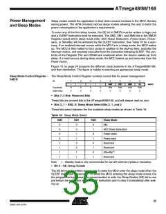
ATmega48/88/168
will contribute significantly to the total current consumption. Refer to “Brown-out Detec-
tion” on page 43 for details on how to configure the Brown-out Detector.
Internal Voltage Reference
The Internal Voltage Reference will be enabled when needed by the Brown-out Detec-
tion, the Analog Comparator or the ADC. If these modules are disabled as described in
the sections above, the internal voltage reference will be disabled and it will not be con-
suming power. When turned on again, the user must allow the reference to start up
before the output is used. If the reference is kept on in sleep mode, the output can be
used immediately. Refer to “Internal Voltage Reference” on page 45 for details on the
start-up time.
Watchdog Timer
Port Pins
If the Watchdog Timer is not needed in the application, the module should be turned off.
If the Watchdog Timer is enabled, it will be enabled in all sleep modes and hence
always consume power. In the deeper sleep modes, this will contribute significantly to
the total current consumption. Refer to “Watchdog Timer” on page 46 for details on how
to configure the Watchdog Timer.
When entering a sleep mode, all port pins should be configured to use minimum power.
The most important is then to ensure that no pins drive resistive loads. In sleep modes
where both the I/O clock (clkI/O) and the ADC clock (clkADC) are stopped, the input buff-
ers of the device will be disabled. This ensures that no power is consumed by the input
logic when not needed. In some cases, the input logic is needed for detecting wake-up
conditions, and it will then be enabled. Refer to the section “Digital Input Enable and
Sleep Modes” on page 66 for details on which pins are enabled. If the input buffer is
enabled and the input signal is left floating or have an analog signal level close to VCC/2,
the input buffer will use excessive power.
For analog input pins, the digital input buffer should be disabled at all times. An analog
signal level close to VCC/2 on an input pin can cause significant current even in active
mode. Digital input buffers can be disabled by writing to the Digital Input Disable Regis-
ters (DIDR1 and DIDR0). Refer to “Digital Input Disable Register 1 – DIDR1” on page
230 and “Digital Input Disable Register 0 – DIDR0” on page 245 for details.
On-chip Debug System
If the On-chip debug system is enabled by the DWEN Fuse and the chip enters sleep
mode, the main clock source is enabled and hence always consumes power. In the
deeper sleep modes, this will contribute significantly to the total current consumption.
39
2545D–AVR–07/04

 ATMEL [ ATMEL ]